
Based on AVS technology to maximize energy saving of multimedia mobile phone processor
User experience is very important for end users, and network operators and content providers also rely on these new multimedia functions and their extended services to generate revenue, so limited battery life means limited revenue.
The current power conversion efficiency has exceeded 90%, and the further improvement of efficiency will have little impact on the whole. Therefore, it is necessary to adopt new technologies for system-level energy management. If the processor can adjust the frequency according to actual needs, and combined with the power management technology that can reduce the voltage according to the frequency, it can significantly reduce energy consumption and extend the running time accordingly.
Voltage regulation
The concepts of voltage regulation and energy saving can be expressed by the energy consumption formula of the digital system:
E = {(CVDD2f) + (VDDILEAK)} t
Here the dynamic terms include C (circuit capacitance), VDD (power supply voltage) and f (clock frequency); the static terms are determined by the ILEAK (leakage current) of the digital gate circuit. From this formula, it can be seen why the use of common energy-saving techniques in digital circuits can ultimately reduce energy consumption by reducing the frequency (f) and voltage (VDD) of the processing engine. Dynamic voltage regulation (DVS) and adaptive voltage regulation (AVS) are two commonly used voltage regulation techniques. Figure 1 shows the energy savings achieved by DVS and AVS.
What are DVS and AVS?
DVS is an open-loop scheme that adjusts voltage and frequency by pre-characteristic reduction or using a voltage-frequency lookup table. These voltages must be high enough to maintain functionality across all devices and temperature ranges. Although this open-loop scheme can save considerable energy, it cannot achieve all possible energy savings.
AVS is a closed-loop solution, which can complete the task in time while reducing the power supply voltage as much as possible. DVS adjusts the power supply voltage to a fixed pre-characteristic value, while ignoring changes in process, temperature, and power supply. AVS takes all these factors into account when determining the optimal supply voltage to ensure that energy consumption is minimized.
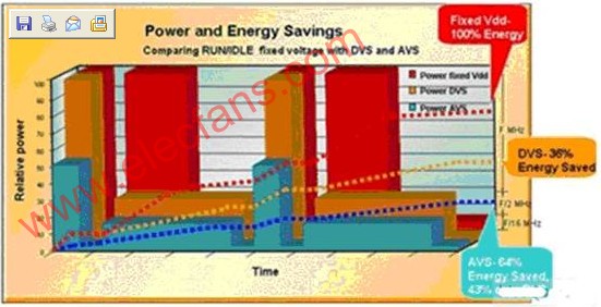
Figure 1: Compared with fixed voltage operation mode, the energy saving achieved by DVS and AVS technology.
How AVS works
AVS is a system-level solution that can independently control the power supply voltage of each processing engine in the SoC, thereby reducing the energy consumption of the digital SoC solution. AVS embeds a comprehensive core compatible with the Advanced Microcontroller Bus Architecture (AMBA) and an advanced power controller (APC) in the SoC, as shown in Figure 2.
APC enables the system to achieve dynamic voltage regulation or fully adaptive voltage regulation on the target SoC. APC interacts with the power supply system to reduce power requirements while maintaining peak efficiency to ensure that the power supply voltage at the current SoC clock frequency is minimized, thereby minimizing digital logic energy consumption.
APC uses three interfaces to connect the rest of the system: an AMBA-compatible host interface, a clock management unit (CMU) interface, and an open standard PowerWise interface (PWI). The host interface is used to control and configure APC2, while the CMU interface is used to coordinate changes in voltage and frequency.
PWI is a simple and fast (up to 15MHz) two-pin serial interface, specifically designed to meet the requirements of AVS and DVS, and has a wide range of programming options to suit multi-purpose applications. The latest PWI 2.0 standard supports multiple SoCs and peripherals on the same bus. The PWI interface is used to communicate power management information with an external energy management unit (EMU) or control other peripherals.
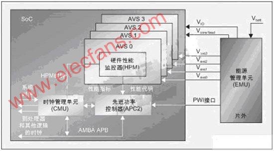
Figure 2: AVS implementation plan.
Summary of this article
With the emergence of more and more media content and high-speed data rates, how to perform high-speed processing in multimedia phones while saving energy to extend battery life is becoming a challenge. Advanced power management technologies such as AVS can greatly reduce the energy consumption of digital processing, thereby extending device runtime and enhancing user experience. Using these advanced energy-saving technologies eliminates the need to charge the battery every few hours, extending the phone's talk time, game time, or video time. Therefore, these technological advancements allow us to enjoy more mobile services.
8" Novelty Candle have 22g 23g 25g sell very well for Jeddah market . 8" Novelty Spiral Candle can do your own brand and logo .boxes. each box have 12pcs, each carton have 24boxes. Novelty Scented Candles have many colors , such as white , yellow ,green ,blue ,red and so on . we are the biggest CANDLE FACTORY IN hebei province , We make sure the shipment is quick . usually about 30-35days after receiving the deposit and confirming the package .
Welcome to inquiry and welcome to order !
8" Novelty Candle
8" Novelty Candle,8" Novelty Spiral Candle,Novelty Scented Candles,Glass Jar Novelty Candles
Shijiazhuang Zhongya Candle Co,. Ltd. , https://www.zycandlefactory.com