There are various causes of EMI in PCBs, including RF currents, common-mode signals, ground loops, impedance mismatches, and magnetic flux. To effectively manage EMI, it's essential to gradually understand these factors and their impact on the system. While electromagnetic theory provides the mathematical foundation for EMI phenomena, it can be complex and time-consuming to grasp. For most engineers, a clear and practical explanation is more valuable. This article explores the "source of electricity" on a PCB, the application of Maxwell’s equations, and the concept of minimizing magnetic flux.
**Source of Electricity**
Unlike magnetic sources, electric sources are modeled using time-varying electric dipoles. This means there are two closely spaced, oppositely charged points that change over time. The current flowing through this dipole generates an oscillating charge distribution. An oscillator driving an unterminated antenna is a good example of such a source. However, this circuit cannot be fully analyzed using low-frequency circuit principles because the signal propagation speed is limited by the dielectric material. As a result, RF currents can develop in the circuit.
The electromagnetic field produced by this source depends on four key factors:
1. **Current Amplitude**: The strength of the electromagnetic field is directly proportional to the current flowing through the dipole.
2. **Polarity Relationship**: The polarity of the dipole must match that of the measuring device's antenna for accurate detection.
3. **Size of the Dipole**: The field strength increases with the length of the dipole, but only up to a certain fraction of the wavelength. Larger dipoles tend to resonate at lower frequencies.
4. **Distance from the Source**: Both electric and magnetic fields decrease with distance. In the far field, the behavior resembles a loop source, producing a plane wave. Near the source, the field strength decreases more rapidly with distance.
The relationship between near-field and far-field components is illustrated in Figure 1. All electromagnetic waves consist of both electric and magnetic field components, forming what is known as the Poynting vector. A single radio wave or magnetic wave does not exist—what we measure is a combination of both. For small antennas, the wavefront appears flat at a few wavelengths away from the source.
The unit of electric field strength is volts per meter (V/m), while the magnetic field is measured in amperes per meter (A/m). The ratio of these fields represents the free-space impedance, which is approximately 377 ohms and remains constant regardless of distance or source characteristics.
In most applications of Maxwell’s equations, noise coupling can be modeled using equivalent components. A time-varying electric field between two conductors represents a capacitor, while a time-varying magnetic field corresponds to mutual inductance. These mechanisms are shown in Figure 2.
**Plane Wave Behavior**
For the lumped-component model to be valid, the circuit size should be much smaller than the signal wavelength. If this isn’t the case, the model may not be accurate. However, even when the model is approximate, it still offers valuable insights into EMC behavior for several reasons:
1. Maxwell’s equations are difficult to apply directly due to complex boundary conditions. Lumped models, although simplified, are often reliable and widely used.
2. Numerical models may not clearly show how noise is generated based on system parameters. The lumped component approach provides better insight into system behavior.
Understanding Maxwell’s equations is crucial for PCB design and layout. It helps engineers identify how electromagnetic fields are created and how to reduce unwanted radiation. This involves managing RF currents, which are linked to signal distribution, bypass capacitors, and coupling. Minimizing the loop area of return paths in the signal network reduces EMI. Bypass and coupling also play a role, as they can lead to large currents in the power distribution network, increasing RF loop areas.
Figure 3 illustrates the noise coupling methods discussed above. By applying these principles, designers can significantly improve the electromagnetic compatibility of their PCBs.
Benchtop DC Power Supplies
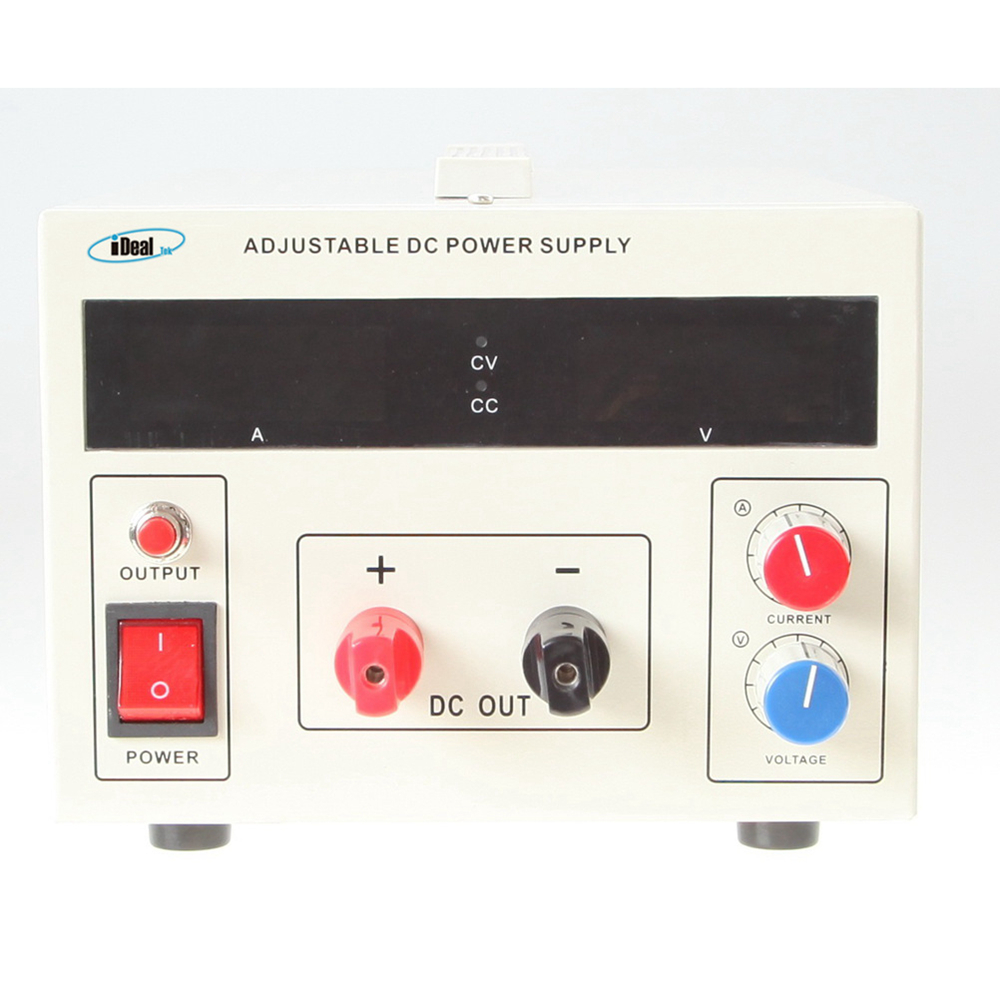
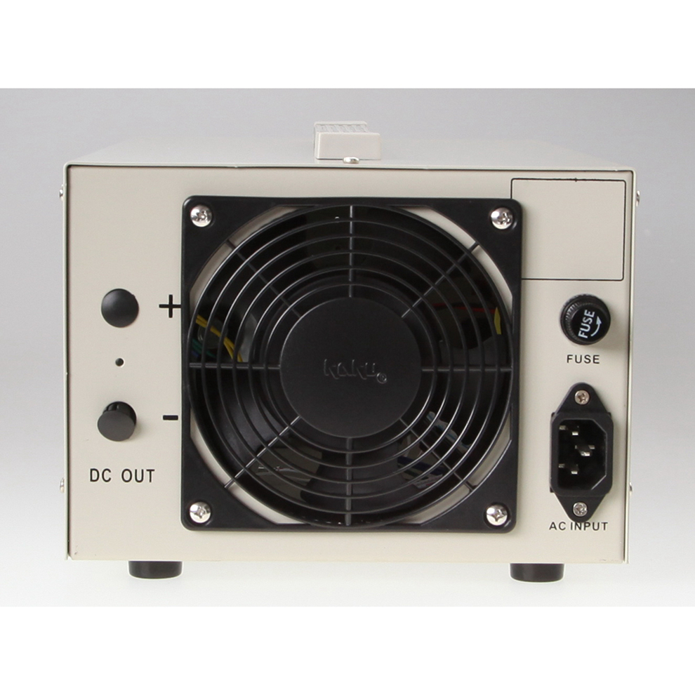
SMP series Bench DC Power Supplies are economical, MOSFETs-based, high switching speed, high power density desktop DC power supplies with output power covering 300W ~ 6KW, and maximum voltage up to 800VDC.
Compared with IGBT-based DC switching power supplies, MOSFET-based switching power supplies have a higher switching frequency, making this series Benchtop DC power supplies can use smaller semiconductor devices and LC filter units while ensuring low ripple, high precision, and fast response characteristics of the Benchtop Laboratory Power Supplies DC output. Which gives more space to use a smaller chassis size at the same output power, resulting the high-power density feature of this series Benchtop AC DC power supplies.


The main design purpose of this series of Bench AC-DC power supplies is to fulfill the needs of small laboratory test, precise experiment and universities.
At present, this series of Bench AC DC power supplies below 1KW adopts desktop chassis to match laboratory applications, they are mainly used in LED testing, small electroplating, heating of new materials, electrical component testing and other applications.
Bench DC Power Supplies, Desktop DC Power Supplies, Bench Laboratory Power Supplies, Benchtop AC DC Power Supplies, Bench AC-DC Supplies
Yangzhou IdealTek Electronics Co., Ltd. , https://www.idealtekpower.com


