
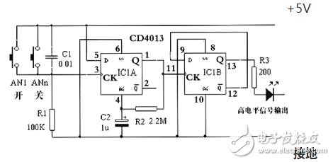
CD4013 integrated circuit signal transmission characteristics and application circuit (multi-ground control light switch)
Simple Multi-Control Switch Circuit Using CD4013
This circuit is designed as an energy-saving lamp control system. When going upstairs, pressing AN1 turns on the light (H). Once you enter the room, pressing IN turns it off. Unlike traditional monostable energy-saving lamps, this circuit allows for arbitrary time intervals between pressing AN1 and ANn, without being restricted by timing or spatial constraints.
Control Schematic:
Application Control Circuit:

Signal Transmission Characteristics of CD4013 – Part 1:
When a high level is applied to pin 3 (CK) of the CD4013, the first pin (Q) outputs a high level. Similarly, when a high level is input to pin 11 (CK), the 13th pin (Q) outputs a high level.
Signal Transmission Characteristics of CD4013 – Part 2:
The CD4013 is a dual D-type flip-flop IC. Each flip-flop has a set terminal (SET), reset terminal (RESET), clock terminal (CLOCK), data input terminal (DATA), and two output terminals Q and Q̅ (inverted Q). It operates within a voltage range of 3–18V.


Function Description:
When R = 1 and S = 0, regardless of the state of D and CLK, the output Q must be 0. This makes R the reset terminal. When S = 1 and R = 0, the output Q becomes 1, making S the set terminal. If both R and S are 0, the output Q follows the D input at the rising edge of the CLK signal. For example, if D = 1, then Q = 1, and if D = 0, then Q = 0.

Pressing S1 sets R = 1, resetting the circuit and causing Q to go low. Pressing S2 sets S = 1, which triggers the circuit to set Q to high. When Q is high, the transistor turns on, energizing the relay. The relay remains activated until S1 is pressed again. This forms a basic RS flip-flop circuit.

When S1 is not pressed, R = 0, allowing the circuit to remain in its steady state. If S1 is pressed, the CP terminal transitions from low to high, triggering the D input to be transferred to Q. Since D = 1, Q becomes high, entering a transient state. The capacitor C charges through R2, and once it reaches the reset threshold, R = 1, resetting Q back to low. This cycle controls the delay before the light turns off, depending on the values of R2 and C.

After power-on, the Q terminal is set to high. The high voltage charges C2 through RP2. When the voltage across C2 reaches the reset threshold, Q goes low, and C2 discharges through VD2. At this point, QÌ… becomes high, charging C1 through RP1. As C1 reaches the set threshold, the circuit resets, and Q goes high again. This creates a continuous oscillation between high and low levels at Q and QÌ…, forming an oscillator. The oscillating signal at Q is amplified by a transistor and used to drive a speaker, producing an audio tone. The frequency of the oscillation depends on the values of RP1, RP2, C1, and C2.


The AC 220V supply is rectified by VD1–VD4, limited by R1, filtered by C1, and regulated by VS to provide +12V for the control and actuation circuits. During the day, RG1 and RG2 are exposed to light, keeping their resistance low. This results in a low level at the S1 input of the IC, turning off the transistor VT and keeping the relay K released, so the lamp EL remains off. At night, when RG1 and RG2 are dark, the S1 input goes high, causing the R1 terminal to go low, setting Q1 high. This activates the transistor VT, energizing the relay K and closing its normally open contacts, lighting the lamp EL. As daylight returns, the resistance of RG1 and RG2 decreases, turning off the lamp again.
YIWU JUHE TRADING COMPANY , https://www.nx-vapes.com