
GPS receiver design using SiGe process (1)
Based on the Federal Communications Commission's (FCC) E911 Orientation and Location Service (LBS), it is expected that Global Positioning System (GPS) receivers that follow this standard will be ready to play a vital role in wireless communications. Successful E911/LBS products and services will require solutions with the following features: GPS functionality in mobile phones, low cost, low power consumption, high accuracy, high sensitivity and good immunity.
GPS receivers typically include two functional blocks: a radio frequency front end and a baseband digital signal processor (DSP). Today, with the development of CMOS digital technology, baseband processing designs have been allowed to be transferred to semiconductor manufacturers, using system cores such as CEVA's DSP core. Ideally, the RF front-end can also be implemented using standard manufacturing processes and can be transferred to various manufacturers.
This article refers to the address: http://
Support for embedded GPS solutions includes the development of a method to properly provide silicon-based GPS on a radio frequency integrated circuit (RF IC) solution with minimal redesign time. The method is explained next and discusses how to use the software model approach to evaluate RF IC design on Agilent's Advanced Design System (ADS) simulator.
Wireless receiver design is usually divided into two areas: top-level or system-level requirements design, such as chip gain and frequency planning; and separate circuit module performance design. In the traditional design method, different design tools are used for system design, DSP design and RF design. RF IC designers typically must coordinate the different simulation results of analog, digital, and RF signals in high-density circuits. For example, integrating bipolar transistors with passive components and high-speed CMOS logic can cause significant uncertainty in the operation of the circuit, as illustrated by the need to simulate a phase-locked loop (PLL). Co-simulation of the digital counter/divider and analog voltage controlled oscillator (VCO) is required.
The initial design and development of GPS wireless devices required a careful design process with a focus on the specificity and clarity of the target process technology. Transforming it into intellectual property (IP) for application to other design processes requires a way to significantly reduce development time and expense over the initial design phase. Indeed, the vast majority of consumer products have a very short development time, usually only 50 to 70% of the time required for the initial demonstration design.
Therefore, there is a need for a method that supports both frequency domain and hybrid domain simulation techniques; optimization and statistical design tools; and additional equipment, systems, and behavioral models. This approach allows top-down design methods and bottom-up design methods so that transistor-level changes produced by different processor models can be transferred to the system level. ADS allows simultaneous use of time domain and harmonic balance nonlinear simulation techniques.
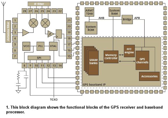
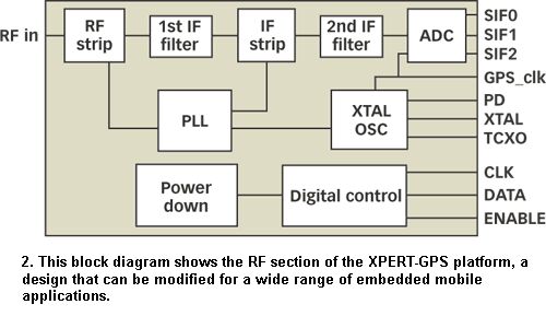
The method enables a trade-off between single-chip GPS receivers with advanced 0.13 μm CMOS processes and advanced designs and separate RF and digital chips (allowing integration of digital intellectual property into the main chip). Software used to help determine overall system performance benefits from a split wireless device based on an advanced SiGe (SiGe) BiCMOS process (Figure 1). The wireless device design refers to the XPERT-GPS RF platform (Figure 2), which provides a wireless RF front end for GPS for mobile communications, such as cell phones and personal digital assistants (PDAs).
For high integration, less than 1.5dB noise figure, low power consumption and low system cost, the wireless design uses a SiGe two-level CMOS (SiGe BiCMOS) process. The wireless device downconverts the GPS L1 band to 1575.42 MHz and completes an optional 1b symbol/amplitude or 2b symbol/1b amplitude analog-to-digital (ADC) conversion to produce a 3.78 MHz baseband signal that is fed into the baseband signal. Baseband processor.
A variable frequency design using an external temperature compensated crystal oscillator (TCXO) provides the essential local oscillation (LO) frequency and baseband clock frequency that can be supported from a single 10 to 26 MHz with a single board design Reference clock frequency. Alternatively, for low cost applications, a single crystal can be used in a device that uses a built-in oscillator circuit.
The key challenge of the RF subsystem is to meet the requirements of GPS image rejection while having two operational capabilities in a mobile phone handset. Good co-processing capabilities must be provided in mutually adverse RF environments, as well as during optimization, including scarce space resources, bandwidth, power, processing power, and per second in the presence of interference in the mobile protocol. Millions of instructions (instruction cycle is clock cycle).
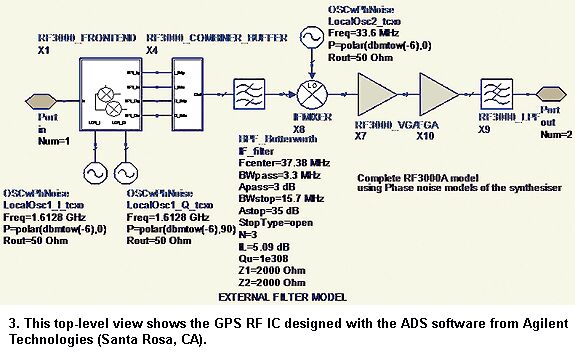
A GPS RF model was developed using ADS at multiple levels of abstraction to generate and transmit GPS signals to a single-channel baseband correlator for demodulation. With this approach, the performance of each module can be defined, optimized, and specified during the silicon process implementation, simplifying the transfer of design to other semiconductor processes. The method also allows RF IC intellectual property to be used as a CEVA module in the customer test platform, thus reducing the time it takes to simulate and extract performance parameters in a given system environment.
Figure 3 shows the top-level schematic of the RF IC in the design simulator window. The emulator allows the display of the characteristics of each module so that the simulated environmental parameters can be easily observed. This is important because each symbol may contain sub-level information.
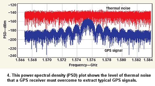
The simulator must be able to simulate key system performance parameters including noise, linearity, gain, sensitivity, frequency, and modulation. Figure 4 shows the power spectral density (PSD) and thermal noise of a representative GPS spectrum. Note the sigma function (sinx/x) characteristic of the GPS signal. The RF IC must be able to handle signals that are approximately 20 dB lower than the noise level, and only by integration until the signal-to-noise ratio (SNR) is greater than zero, the receiver can recover the GPS signal from noise.
Other capacitors
Other Capacitors,Ac Filter Capacitor,Power Saver Capacitor,Line Filter Capacitor,Low Voltage Capacitor
YANGZHOU POSITIONING TECH CO., LTD. , https://www.cnpositioning.com