
Large-scale RF integration reduces handset board area and power consumption
In today's wireless devices, more than half of the components on the board are analog RF devices, so an effective way to reduce board area and power consumption is to implement larger-scale RF integration and move toward system-on-chip. This paper introduces the current status of RF integration development and proposes solutions and solutions for some of these issues.
A few years ago, the cellular handset market dominated single- and dual-band single-mode handsets, using only one or two cellular bands, using the same modulation method, multiple access schemes and protocols in all supported bands. . In comparison, today's next-generation cellular phone design is much more complicated, providing multi-band, multi-mode support, Bluetooth personal area network, GPS positioning and other functions, and ultra-wideband and TV reception functions have begun to appear, in addition to Applications such as games, images, audio and video have also become very common in mobile phones.
Wireless telephony is becoming a complex device called the so-called handheld personal entertainment center, and its development trend is constantly bringing more challenges to designers. Although the new generation of mobile phones has experienced significant growth in communication processing, application processing, number of RF interfaces, and integrated memory capacity compared to voice-only handsets, users still expect mobile phones to have smaller, streamlined shapes. And low price, and a large color display, can provide similar standby and talk time as traditional voice phones. Maintaining the existing form factor and power consumption while exponentially increasing functionality while maintaining overall system cost remains a major challenge for system designers.
Obviously, the problem involves all parts of the overall system design, as well as all wireless communication and entertainment content providers. One area that is particularly effective in reducing board area and power consumption is the RF portion of wireless system design, because in today's typical mobile phones, more than half of the components on the board are analog RF components that are added to Together, they account for 30-40% of the entire board area. Adding RF systems such as Bluetooth, GPS and WLAN will also greatly increase space requirements.
The solution was to do larger-scale RF integration and eventually evolve into a fully integrated system-on-a-chip. Some designers put analog-to-digital converters into the antenna to reduce the total board space required for RF functions. When semiconductor integration technology can integrate more functions in a single device, the number of discrete devices is used to accommodate these devices. The board space is reduced accordingly. As the industry moves toward system-on-chip integration, designers will continue to discover new technologies to meet the conflict between higher RF complexity and longer battery life in small wireless devices.
RF Integration Development Status An important development in RF integration emerged about three years ago when the development of RF technology and digital baseband modems made it possible to replace superheterodyne RF devices with direct downconversion receivers in wireless handsets. Superheterodyne RF devices have been well-applied for many years using multi-stage mixers, filters, and multiple voltage-controlled oscillators (VCOs), but the integration of direct-conversion RF devices can significantly reduce the overall component count of GSM RF. In the late 1990s, a typical single-band superheterodyne RF subsystem including PA, antenna switch, LDO, small-signal RF, and VCTCXO required approximately 200 discrete components; today, we can design a quad-band function The direct conversion system integrates VCO, VCXO and PLL loop filters with less than 50 components.
This article refers to the address: http://
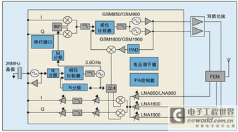
For example, Texas Instruments' GSM transceiver TRF6151 (Figure 1), integrated functions include on-chip voltage regulator, VCO and VCO tank, PA power control, PLL loop filter EDGE blocker detection, LNA gain step control And VCXO.
For designers, advanced integration helps overcome some of the biggest challenges in wireless RF, the most basic of which is the transceiver's DC power supply and its regulation. During a call, the battery voltage changes as temperature and time change. In addition, the noise coupling from the TX VCO and RX VCO power supplies can affect the performance of the entire system, so designers are faced with how to solve the RF board regulator and large The problem with most related passive components. Integrating these devices into the RF transceiver means that the only external component required is a simple decoupling capacitor. This direct connection to the power supply not only simplifies the design but also saves board space.
Another challenge faced by RF designers is the VCO tuning range and lock-in time. In all analog VCO designs. Because it is often necessary to balance the lock time and tuning range, the loop filter is typically placed outside the chip. Sometimes this can be addressed in the software control of the VCO tuning range, however this approach places additional resource requirements on the overall development of the phone. When the digital tuning function is included in the VCO and self-calibration is available, an extended tuning range is available and the loop filter components can be placed in the chip. Obviously, this solution allows design engineers to simplify their work.
In order to obtain the transmitter power control required by the GSM system, PA manufacturers generally include this function in the Power Amplifier Module (PAM). The power controller typically consists of up to several thousand digital CMOS gates, fabricated in a separate chip within the PAM, which increases the cost of the PAM by $0.30 to $0.40. Integrating this functionality into RF devices will eliminate the need for GaAsPAM manufacturers to purchase digital CMOS circuits and load them into PAMs. For an OEM that produces thousands of products per month, removing this extra component will greatly reduce it. Their cost.
Another area where advanced integration can bring substantial savings is VCXO. In the past, expensive VCTCXO modules were purchased as discrete components in RF devices, so the integration of common components of VCTCXO modules into RF devices can reduce cost and related design issues. The TRF6151 requires only a low-cost crystal and variable volume. The diode can perform the function of the VCTCXO.
Despite these integrations and design simplifications, RF design engineers still face difficult choices, one of which is input sensitivity and RX power consumption. It is well known that the larger the current used in a low noise amplifier (LNA) design, the lower the overall noise characteristics. The design engineer must determine the total power budget of the receiver and the receiver sensitivity level requirements. But the noise does not decrease with the power reduction, in fact the opposite. So while meeting the GSM standard, designers must often ask themselves whether it is worth the cost of power consumption to achieve a certain level of sensitivity. This question also explains why it is necessary for design engineers and IC manufacturers to work closely together throughout the design process. Feedback from design engineers can lead IC manufacturers to better serve the wireless industry as they develop future RF products.
The development of SoCs to reduce the cost, power and complexity of wireless systems is critical to successfully meeting system integration requirements. However, developing a highly integrated mobile phone solution requires the semiconductor industry to overcome complex technical barriers that are rarely designed. People care because many of them don't want to know how SoC devices are made, as long as they provide the required performance. Therefore, it is necessary to have a quick understanding of some process technologies that will affect the capabilities and usability of devices used in cellular handset integration.
There are several possible solutions for the integration of mobile phone RF electronic systems. First, a traditional RF architecture can be implemented in a relatively simple bipolar or BiCMOS process using conventional techniques. The final RF chip can be assembled with the digital logic functions of the handset using multi-chip packaging technology (system-in-package technology). While this technology has many advantages, such as the familiar RF design approach and proven processes and technologies, the high cost and yield limitations of test devices make it difficult to commercialize.
There is also a method in which mobile phone electronic system integration can also be obtained using an advanced BiCMOS (SiGe) wafer process. However, due to the additional lithography process required to process SiGe HBT devices, the final chip will require an additional cost, and because SiGe BiCMOS technology cannot utilize state-of-the-art lithography processes, BiCMOS processes are often lagging behind advanced digital CMOS processes. These will put a lot of pressure on adding handset features and reducing costs. It can't be solved with a simple wafer process strategy, because this technology can't keep the logic or digital part of the system at the lowest possible price at all times, so Monolithic integration of the RF portion of the system baseband function in BiCMOS (or SiGe) is not a good choice.
The final solution that can be considered is RF integration in CMOS, which is also a considerable challenge. Although there are several CMOS cellular RF designs, these designs are largely based on analog functionality. It is difficult to implement analog mixers, filters, and amplifiers in CMOS technology, and the power consumption is generally greater than the SiGe BiCMOS scheme. As process technology advances, CMOS ratings are getting lower and lower, making analog design more difficult. Early in the development of new processes, device modeling and process maturity generally failed to meet the high-precision parametric modeling requirements required for analog module design. However, the recently developed digital CMOS RF architecture makes monolithic CMOS integration more attractive. .
These solutions are also driving the semiconductor industry forward as manufacturers seek low-cost RF system-on-chip solutions. Despite the difficulty of each integration solution, it is truly surprising that RF component integration can reach such a high level. Overcoming these difficulties will make wireless handset design a big step forward and set the direction for greater integration in the near future.
The conclusions of this paper still have many difficulties in RF integration. Every RF device in modern mobile phones faces stringent performance requirements. The sensitivity requirement is about -106dBm (106dB below 1mW) or higher, and the corresponding level is only a few microvolts. In addition, the selectivity is also useful. The rejection of adjacent bands (commonly referred to as blocking) should be on the order of 60 dB; in addition, the system oscillator is required to operate at very low phase noise to prevent folded blocking energy from entering the receive band. RF integration is very difficult due to the very high frequency and extremely demanding performance requirements.
Handling multiple frequency standards poses a real challenge for the entire SoC frequency, hoping to mitigate the excitation generated by in-band signal transmission, and integrating digital RF integration involves much more than placing multiple RF components in a single chip. There needs to be a new architecture for hardware sharing.
For system designers, today's simple, highly integrated, cost-saving semiconductor devices can significantly reduce design complexity while at the same time enriching the characteristics of wireless devices while maintaining system size, battery life and cost. The new highly integrated RF devices also eliminate some of the controversy in wireless design and save engineers valuable time.
PVC insulated wires are coated with pvc to prevent from electric shock. Its light weight reduces manual handling difficulties. This wire consists of copper/aluminum conductor, insulated with moisture and heat resistant, chemically cross-linked polyethylene insulation. PVC does not conduct electricity and is therefore an excellent material to use for electrical applications such as insulation sheathing for cables. With fine design and high quality, the wire boasts of large electricity transmission capacity. The maximum continuous operating temperature for general type is 75℃. But the special type BV-105 can work well at the temperature of 105℃.
Standard:
GB/T5023-2008, JB/T 8734-2016

Rated Voltage:
450/750V

Application:
cables are extensively used for domestic home appliances wiring, house wiring and internal wiring for lighting circuits in factories, power supply for office automation, in control, instrumentation, submarine, mining, ship wiring applications etc. due to its high tensile strength, superior conductivity, better flexibility and ease of jointing.


Advantages:
- A non-hygroscopic insulation almost unaffected by moisture.
- Non-migration of compound permitting vertical installation.
- A tough and resilient sheath with excellent fire retarding quality.
- High current and short circuit current rating.
- Not affected by vibration.
- Reduce internal stress and low dielectric loss
- Complete protection against most forms of electrolytic and chemical corrosion.
- Good ageing characteristics
- Easy installation
Welcome to visit our factory to learn more about us. If you have any questions, please feel free to contact us.
PVC Insulated Wire,Heat Resistant PVC Insulated Wires,PVC Insulator Sheath Electrical Wires,Flexible PVC Electrical Wires
Fujian Lien Technology Co.,Ltd , http://www.liencable.com