
Design of a new supercapacitor energy management system for electric vehicles
The energy management system consisting of supercapacitor and battery takes into account the high power density of the supercapacitor and the high energy density of the battery, which can better meet the requirements of the starting and accelerating performance of the electric vehicle and improve the recovery efficiency of the braking energy of the electric vehicle. Increase driving range.
1 System Overview The supercapacitor and battery energy management system is mainly composed of BLDCM drive controller and bidirectional DC-DC circuit. The system block diagram is shown in Figure 1.
This article refers to the address: http://

In Figure 1, L, M1, and M2 form a bidirectional DC-DC circuit, and VT1 to VT6 form a three-phase inverter, and a high-end load switch M3 is used to control the on and off of the bus and the battery when necessary. The battery bus voltage is Vin=72 V, the supercapacitor is rated at 165 F/48 V, and the brushless DC motor is 72 V/5.5 kW. When the motor is running, the load switch M3 is turned on, the three-phase inverter works normally, the bidirectional DC-DC does not work, the system energy comes from the battery; when the motor energy feedback brake, the bus voltage is higher than the battery voltage and passes the comparator C1 signal. Trigger off load switch M3, bidirectional DC-DC works in BUCK state, super capacitor is charged; when motor starts or large torque output, bidirectional DC-DC works in BOOST state, which usually only lasts for tens of seconds. When the supercapacitor energy is sufficient, the BOOST output voltage can be guaranteed to be higher than the bus voltage, and the load switch M3 is turned off. If the discharge time is too long, since the super capacitor does not have constant voltage characteristics, as the energy is consumed, the terminal voltage will continuously decrease, and the output voltage of the corresponding BOOST circuit will also decrease accordingly. When the output voltage value is smaller than the bus voltage value, the high-side load switch M3 is turned on, at which time the battery is separately powered by the system and the bi-directional DC-DC circuit of the super capacitor portion is turned off.
2 system working principle and control strategy
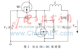
2.1 Bidirectional DC-DC principle The reason for using the bidirectional DC-DC converter in this system is as follows: (1) The supercapacitor terminal voltage and the battery voltage do not match; (2) The supercapacitor does not have constant voltage characteristics, and cannot be inconsistent with the battery voltage characteristics. Put the two together directly. The system uses a supercapacitor rated at 48 V and a battery rated voltage of 72 V, so the low-side voltage of the bidirectional DC-DC converter is 48 V and the high-side voltage is 72 V. Since the voltage conversion range is not large, it is not necessary to use a transformer for voltage conversion, and the PWM chopping can be directly used. The bidirectional DC-DC structure is shown in Figure 2.
The bidirectional DC-DC converter in Figure 2 is essentially a combination of a basic BUCK circuit and a BOOST circuit [1], replacing the power diode in the BUCK circuit or the BOOST circuit with a power MOSFET to obtain the circuit topology shown in Figure 3. . The circuit operates in BUCK buck mode or BOOST boost mode depending on the direction of energy flow.
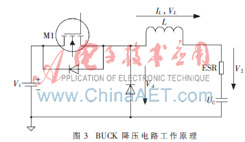
In the BUCK step-down mode, the M1 tube is used as a switching tube, the driving signal is from the PWM control chip; the M2 tube is used as a diode, and the parasitic body diode of the M2 tube is used, and the M2 must be reliably turned off by the negative voltage. Reliable operation of the circuit. The setting circuit works in CCM mode, and the equivalent circuit in buck mode is shown in Figure 3. The arrows in Fig. 3 indicate the direction of voltage and current, and the energy flows from V1 to V2, that is, the charging mode of the super capacitor. The time period from t0 to t1 indicates that M1 is on, and the time period from t1 to t2 indicates that M1 is off. Let the PWM period be T and the duty ratio be D. Then the M1 turn-on time is DT, and the M1 turn-off time is (1-D)T. According to the principle of the volt-second balance of the inductor, the average value of the volt-second value of the inductor L in one cycle is 0, and the average value of the volt-second of one cycle of the inductor can be obtained by the following formula: 
In the BOOST boost mode, the M2 tube is used as a switching tube, the driving signal is from the PWM control chip; the M1 tube is used as a diode, and the parasitic body diode of the M1 tube is used, and the M1 must be reliably turned off by the negative voltage. Reliable operation of the circuit. The setting circuit works in CCM mode, and the equivalent circuit in boost mode is shown in Figure 4. The arrows in the figure indicate the direction of the voltage and current, and the energy flows from V2 to V1, which is the discharge mode of the supercapacitor. The time period from t0 to t1 indicates that M2 is on, and the time period from t1 to t2 indicates that M2 is off. Let the PWM period be T and the duty ratio be D, then the M2 turn-on time is DT, and the M2 turn-off time is (1-D)T. According to the principle of the volt-second balance of the inductor, the average value of the volt-second value of the inductor L in one cycle is 0, and the average value of the volt-second of one cycle of the inductor can be obtained by the following formula: 

Due to duty cycle 0
2.2 Energy Management System Control Strategy and Working Mode
2.2.1 Design requirements The electric vehicle energy management system has high requirements for safety and should meet the following conditions:
(1) Meet the safety requirements of braking and acceleration, in line with the driver's habits. By finding the best coverage of electronic brakes and mechanical brakes, and maximizing energy recovery while ensuring safety, the electric brake process with energy recovery system should be as similar as possible to the traditional brake process; during acceleration, as much as possible More energy is released to ensure the acceleration performance required by the car.
(2) Consider the performance of the energy management system and the motor to ensure the safety of components such as supercapacitors, inductors, motors, etc. during energy feedback and release, avoiding excessive charging or discharging current or excessive charging voltage and damaging components.
2.2.2 Control strategy (1) Energy feedback control strategy In the case of meeting the design requirements (1), the optimal braking force is determined according to the limit value of the requirement (2), so that the recovered energy reaches the maximum, that is, the integration of the current with time reaches maximum. In order to comply with the usual braking habits, the brake pedal is multiplexed with electric brake operation and mechanical brake operation. The whole brake pedal stroke is divided into two sections. The first stroke is the electric brake control section. With the pedal down, the electric brake strength is gradually strengthened. The second stroke is the mechanical brake control section, with the pedal down, the mechanical brake The intensity is gradually strengthened.
The limiting factors are quantified as the current maximum allowable braking torque, and thereby the braking torque of the motor is limited, thereby protecting the normal operation of the system. The limiting factors of electric braking are mainly from two aspects of motor and energy management system, including the maximum allowable braking torque of the motor, the maximum allowable braking power of the motor, the maximum allowable charging power of the energy management system and the maximum allowable charging current of the energy management system. The specific strategies for converting these finite factors into motor torque limits are: 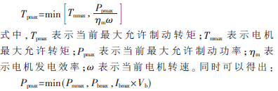
In the formula, each physical quantity is positive; min() represents the minimum value; max() represents the maximum value, Pmmax represents the maximum allowable braking power of the motor; Pbmax represents the maximum allowable charging power of the energy management system; Ibmax represents the energy management system Maximum allowable charging current; Vb represents the terminal voltage of the current energy management system. The two limiting factors of the energy management system and the terminal voltage are variable. The current transient value of the system operation is given by the energy management system. The motor power generation efficiency and the current motor speed are variable, and the current transient value of the motor is taken. It is given by the motor control system.
(2) Energy release control strategy The specific description of the energy release control strategy is similar to the energy feedback control strategy. The limiting factors are quantized to the current maximum allowable driving torque, and the driving torque of the motor is limited to ensure the normal operation of the system.
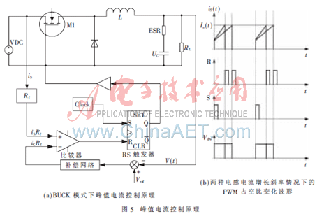
3 Bidirectional DC-DC control method The bidirectional DC-DC control method adopts voltage and current double closed loop control [2], wherein the voltage loop is the outer loop, and the closed loop control of the voltage is realized by the TL431 and the optocoupler; the current loop is the inner loop, and the pair is used. The method of closed-loop control of peak current. Peak current control not only has a fast response, but also has current limiting protection to improve system reliability. The basic principle of peak current control is shown in Figure 5. Figure 5 (a) shows the principle of peak current control in BUCK mode, and the principle of peak current control in BOOST mode is similar. In the figure, the error signal obtained by subtracting the reference voltage Vref from the converter output voltage V(t) is amplified by the compensation network and used as a modulation signal of the PWM modulator, and the current sampling signal is(t)Rf is used as a carrier signal. At the beginning of each switching cycle, the RS flip-flop is set by the clock pulse, and the switching device M1 is turned on, and then the inductor current is gradually increased, as shown in Fig. 5(b). When it is detected that the current signal is(t)Rf is greater than the modulation signal ic(t)Rf, the comparator inverts and resets the RS flip-flop such that the power tube switch is turned off and the inductor current continues to flow through the freewheeling tube. Figure 5(b) shows the PWM duty cycle variation waveform for both inductor and current ramps. The waveform in the figure shows that when the inductance and current increase rapidly (slope is large), that is, when the load is large (for the charging of the super capacitor, it is the initial charging moment, the circuit is close to the short circuit state), the current quickly reaches the peak value, and the circuit is also very The peak current control state is quickly entered, and the duty ratio of the PWM output waveform becomes smaller; on the contrary, the PWM output waveform duty ratio becomes larger.
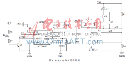
4 Bidirectional DC-DC hardware design In this design, the double-closed loop structure is used to control the current and voltage. The control chip uses TI's UCC3803A. An error amplifier and current amplifier inside the UCC3803A can easily form a double loop of current and voltage. In actual use, in order to have a faster response speed, the error amplifier can be omitted, and the voltage regulator TL431 and the optocoupler PC817 are used to form the voltage feedback. The current loop was built using LEM's current sensor LAH 100-P. The BUCK control circuit is shown in Figure 6, and the BOOST control circuit principle is similar, except that the current direction and the position of the switch tube are changed. IS1 is the voltage measurement signal from the LEM Hall current sensor LAH 100-P output, which enters the current feedback terminal, the ISEN terminal in Figure 6. V48 comes from the output of the power section. Since the TL431 can only be regulated to 36 V at most, it is necessary to partially modify the classic TL431 regulator circuit to meet the 48 V regulation requirements. Therefore, the TL431 has 3 pins (ie, K pole). Introducing a 24 V regulator, the terminal voltage of the TL431 is about 24 V, which can normally regulate the voltage in the safe working area. PC817 achieves electrical isolation and is regulated by the output voltage Vce. When the super capacitor voltage is close to 48 V, the PC817 output current Ic increases, then Vce decreases, and the signal entering the UCC3803's 2-pin VFB compensation terminal is also reduced. Correspondingly, the PWM output duty cycle is also reduced; when the super capacitor voltage exceeds 48 V, the UCC3803 compensation terminal 1 is pulled low, the PWM is turned off, and the overvoltage protection function is maintained. At this time, the circuit will maintain dynamic balance at 48 V. .
The system is currently undergoing experimental verification, stable operation, good energy feedback and release performance.
references
[1] He Yikang, Pan Zaiping. Power Electronics Technology [M]. Beijing: Science Press, 2004.
[2] Xu Dehong. Modeling and Control of Power Electronic Systems [M]. Beijing: Mechanical Industry Press, 2007.
Transparent Screen Protector is engineered for 3X stronger anti-shock
ability, leading strength and durability. 9H hardness guard screen will not get scratched even using hard object such as
knives and keys. In
addition, 2.5D arc edges are smooth to the touch and do not scratch your
fingers. Nano waterproof Oleophobic coating is used on Glass Screen Protector to effectively reduce fingerprint residue.

Pls
feel free to contact us if you are interested in these products, have any
questions or special needed. We have the best sales team to service to you.
Look forward to your inquiry, and welcome to visit our factory.
Transparent Screen Protector
Transparent Screen Protector,Transparent Screen Protector For Iphone X,Cell Phone Screen Protector,Transparent Screen Protector For Iphone 8
Shenzhen Kantou IM Technology Co., Ltd. , https://www.kantou-im.com