MAX16046–MAX16049 EEPROM programmable system management
The MAX16046–MAX16049 EEPROM programmable system manager is a power sequencer, monitor, and margin regulator that can control up to 12 power supplies. The power supply is monitored by three digital comparators, the margin is adjusted by the programmable DAC output, and it is sequenced by the programmable state engine.
The system manager includes an I²C interface compatible with SMBus ™ and a JTAG interface, both of which can access all registers of the device and program internal configuration EEPROM. MAX16046–MAX16049 can be programmed online, and only a few simple rules are required.
The supply voltage range for the MAX16046–MAX16049 is 3V to 14V. In typical applications, connect VCC to a 12V medium voltage bus or 3.3V auxiliary power supply.
The MAX16046–MAX16049 can be programmed using a local power board. For example, a 3.3V auxiliary voltage can be used without any other power supply, or a 12V medium voltage bus can be applied. Since the system manager at this time has not been programmed, all downstream power supplies should be turned off. It is also possible to use a common double diode to supply power from the programming connector. Due to the voltage drop caused by the diode, this method works best when the MAX16046–MAX16049 are powered by a 12V bus.
If you do not use a diode logic OR circuit and program the MAX16046–MAX16049 when the circuit board is powered on, you must pay attention to the state of the sequencing output to prevent the downstream power supply from turning on prematurely.
The MAX16046–MAX16049 are high-impedance outputs before programming. The active-high power enable input should have a pull-down resistor, and the active-low power enable input should have a pull-up resistor. The sequencing output can be set to push-pull output or open-drain output. Because the open-drain configuration requires an external pull-up resistor, only a low-level enable input can be used.
It is best not to connect the MAX16046–MAX16049 to the JTAG link because the upstream devices in the link may not be powered, preventing access to the MAX16046–MAX16049. It is recommended to prefer the JTAG multiplexer or the dedicated JTAG interface.
Shared bus When a device (not µP) needs to communicate with the MAX16046–MAX16049 during normal operation, there is a potential problem. For example, when the system monitoring µP requires access to the MAX16046 ADC reading. When the board is powered off or only partially powered, and the MAX16046 is being programmed, other devices connected to the I²C or JTAG bus may cause interference. The easiest solution is to program the MAX16046 through the JTAG interface and monitor the µP connected to the I²C interface. If µP supports open-drain I²C-bus I / O (ie, no ESD protection diode pin connected to VCC), and the pull-up resistance is large enough, it is feasible to share the I²C-bus only during programming and normal operation. If the µP I²C bus is not open-drain, the ESD diode will clamp the bus and interfere with programming.
If the system µP does not have a true open-drain I²C bus, a circuit similar to Figure 1 can be used to automatically switch between the µP and the programmed I²C bus.
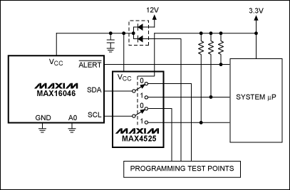
Figure 1. The MAX16046 shares its I²C bus through the MAX4525 multiplexer / switch
The MAX4525 multiplexer shown in Figure 1 switches between the I²C connected to the system µP and the I²C connected to the programming test point. The switch is controlled by the VCC of the system µP. If a 12V power supply is used instead of VCC, the switch connects the I²C to the programming test point. Once VCC power is applied, the switch connects I²C to the system µP.
Application circuit example Three different application circuits for online programming are introduced in the following diagram.
12V medium voltage bus power supply, programming through the I²C bus The circuit shown in Figure 2 supplies power to the MAX16046 through the 12V medium voltage bus, and is monitored by the analog enable terminal EN. When the 12V bus voltage exceeds the threshold set by the resistor divider at EN, if the device has been programmed, the MAX16046 attempts to sequence. The unprogrammed MAX16046 has no response, and the sequencing output remains in a high-impedance state.
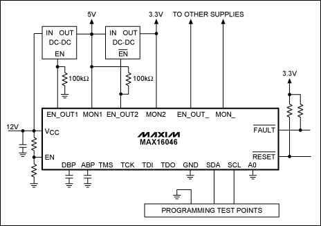
Figure 2. The MAX16046 is powered by a 12V medium voltage bus and programmed through the I²C interface
One power supply uses high-level push-pull enable control, while other power supplies use low-level open-drain enable control. When the unprogrammed output is in a high-impedance state, proper pull-up and pull-down resistors can prevent the power from turning on.
It should be noted that the push-pull output cannot be pulled up to a voltage above VDBP, and the open-drain output cannot be pulled up to a voltage above 6V. The I²C connection is led to the programming test point, and the programming hardware must provide an appropriate pull-up resistor. This circuit is very simple because there are no other devices on the board that need to be connected to the I²C bus.
3.3V auxiliary power supply, programming through JTAG multiplexer as shown in Figure 3, MAX16046 is powered by 3.3V auxiliary power supply. Use a DS26900 JTAG multiplexer to share the JTAG connection with other devices. The DS26900 JTAG multiplexer is also powered by a 3.3V auxiliary power supply. The programming can be completed without applying a 12V medium voltage bus when powered by 3.3V.
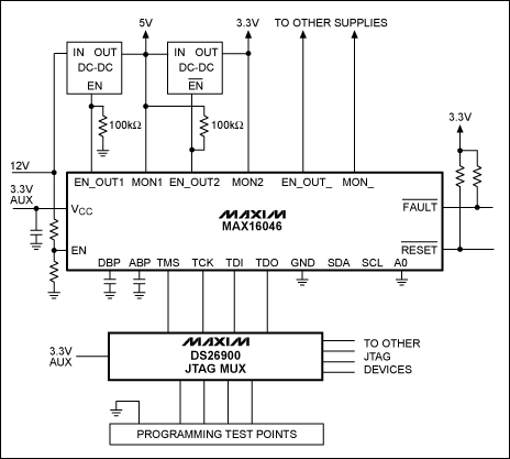
Figure 3. The MAX16046 is powered by a 3.3V auxiliary power supply and programmed by the DS26900 JTAG multiplexer
12V medium bus power supply, as shown in Figure 4 through JTAG programming, MAX16046 is powered by a diode logic OR circuit connected to a 12V medium voltage bus, which can be safely powered without affecting downstream circuits. The JTAG and power connections are led to the programming test point.
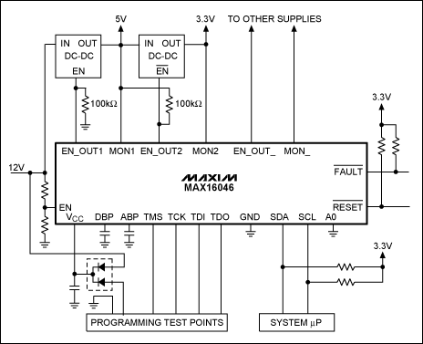
Figure 4. The MAX16046 is powered by a 12V medium voltage bus and programmed via JTAG
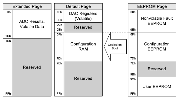
The programming algorithms MAX16046–MAX16049 have built-in EEPROM for storing device configuration parameters. After power on, the content of EEPROM is sent to RAM register. Both RAM and EEPROM can be accessed via JTAG and I²C interfaces. To properly program the MAX16046–MAX16049, the required parameters must be set in EEPROM—see the memory table shown in Table 1.
Table 1. MAX16046 memory table
The configuration file MAX16046 evaluation kit (EV kit) software provides two types of configuration software. One is by selecting File
 A readable XML file generated by Save ConfiguraTIon As, which can be used for I²C programming. The other is by selecting File Save as .SVF generated file, the file is continuous vector format (SVF), third-party JTAG tools and online PCB testing can use this file for JTAG programming.
 The XML file can be viewed in a color-coded layered format on various web browsers. The XML file generated by the EV software is divided into several segments and contains setting tab information and register data. There are two important parts: the Config_Register part containing the configuration values ​​loaded into the EEPROM and the User_Register part containing the loading into the user EEPROM.
In each part, the Register tag specifies the value loaded to a specific address. The format of the register label is:
For more information about the XML file format, please visit the XML Developer Center.
For detailed information on the SVF file format, please refer to Serial Vector Format SpecificaTIon (PDF, 85.2kB).
I²C Programming Procedure When programming the MAX16046–MAX16049 EEPROM configuration memory, you must first determine that the configuration lock bit on register r5Dh [0] is zero. If it is not zero, write "1" to this bit to clear it. To write to EEPROM, you can send the appropriate command, enter the EEPROM page, load the start address, and then send a series of block programming commands. For detailed information about the corresponding I²C protocol, please refer to the data sheet of the MAX16046 / MAX16048 or MAX16047 / MAX16049.
The following is the logic code of a typical EEPROM programming process: SendByte (5Dh) // Check lock bit If ReadByte () & 2 == 2 Then WriteByte (5Dh, 02h) // Clear lock bit if needed SendByte (9Ah) // Access EEPROM page Loop Address from 0Fh to 7Dh SendByte (Address) // Load address WriteBlock (Data, 10h) // Write a block of 16 bytes Wait (16 * 11 milliseconds) // Wait for programming SendByte (Address) ReadBlock (DataRead, 10h) // Read back data block If DataRead! = Data Then RepeatCount = RepeatCount + 1 If RepeatCount == 3 Then Fail Else RepeatCount = 0 Address = Address + 10h // Advance to next block SendByte (9Bh) // Return to default Page Success If you want to write to the user EEPROM, you can use the same procedure, just use the address range 9Ch to FFh instead of 0Fh to 7Dh.
Technical features
1. Preeminent effects: Clear and stable pictures without distortion and disturbance.
2.
quality: adopting first-class chips and wafers imported from abroad
3. Flexible form: continuity, overlying, combination of dynamic and static playing, various effects include rolling moving, typewriting, gradual changing and so on
4. off-line running function: adopting the monolithic design technology and computer string communication way, which can operate in off-line state setting the dates and revising a data via the telephone line
Technical Parameters
Multi language: English/Spanish/Russia/Inter.char.set-..
1)High Brightness, user can change the advertising words whatever you want, easy and convenient in operation, more attactive compared with traditional banner.
2) The led moving sign display supports many kinds of languages and characters.
3) A lot of lively animation icons are built-in. 50 and more action effects for user option; Different brightness can be adjusted in software.
4) Time clock format, support date, countdown and any other odditional functions like temperature and humidity. Voltage input: 220v or110v.
5) led moving sign display Structure: well appreance frame, professional pendents, standard connectors and other accessories.
Usage
Service propaganda in finances, post offices, telecom, commerce, hospitals, sports stadiums
Policies and decrees issued from government organizations
Instructions, guidance and information issuance in airports and railways
Our service
1.Your inquiry related to our products or price will be replied in 24hrs
2.OEM&ODM,any your customized lightings we can help you to design and put into product
3.Protection of your sales area,ideas of design and all your private information
4.Top Quality+Reasonable Price+Responsible After Service=Successful & Win
5.Produce all kinds of Pitch: P4.75, P7.62, P10, P12, P16, P20, P25, P31.25...

Indoor Single Color LED Display
Indoor Single Color Led Display,Led Panel Screen,Single Led Display,Single Color Led Message Display
Shenzhen Joy LED Display Co., Ltd. , https://www.joe-led.com