
High-speed ADC power supply design
Today, designing clean power supplies for high-speed ADCs can be challenging when designers are faced with numerous power options. This is especially important where high efficiency switching power supplies are used instead of traditional LDOs. In addition, most ADCs do not give high frequency power supply rejection specifications, which is a key factor in choosing the right power supply.
This technical article will describe techniques for measuring the AC power supply rejection performance of a converter, thereby establishing a benchmark for converter power supply noise sensitivity. We will perform a simple noise analysis of an actual power supply and show how these values ​​can be applied to the design to verify that the power supply meets the requirements of the selected converter. In summary, this article will describe some simple guidelines to give the user some guidance to help design power supplies for high-speed converters.
Many applications today require high-speed sampling analog-to-digital converters (ADCs) with 12-bit or higher resolutions for users to make more accurate system measurements. However, higher resolution also means that the system is more sensitive to noise. Each time the system resolution is increased by one bit, for example from 12 to 13 bits, the system's sensitivity to noise is doubled. Therefore, for ADC design, designers must consider a source of noise that is often forgotten – system power. The ADC is a sensitive device and each input (ie analog, clock, and power input) should be treated equally to achieve optimal performance as described in the data sheet. There are many sources of noise and various forms, and noise radiation can affect performance.
The buzz concept in today's electronics industry is that new designs are “green†while reducing costs. Specific to portable applications, it requires reduced power consumption, simplified thermal management, maximum power efficiency, and extended battery life. However, most ADC data sheets recommend using a linear power supply because its noise is lower than that of a switching power supply. This may be true in some cases, but new technological developments have proven that switching power supplies can also be used in communications and medical applications (see “How to Test Power Supply RejecTIon RaTIo (PSRR) in anADC†in the References section). Power Supply Rejection Ratio (PSRR) in the ADC)). This article describes the various test and measurement methods that are critical to understanding high-speed ADC power supply designs. In order to determine the sensitivity of the converter to the effects of the supply rail noise and to determine what level of noise the supply rail must be in order for the ADC to achieve the desired performance, two tests are useful: commonly referred to as the power supply rejection ratio (PSRR) and power supply modulation ratio. (PSMR).
Detailed analog power pin
The power pin is generally not considered an input, but it is actually an input. Its sensitivity to noise and distortion can be as sensitive as clock and analog input pins. Even if the signal entering the power pin is actually DC, and there is generally no repetitive fluctuation, there is still a certain amount of noise and distortion on the DC offset. The cause of this noise may be internal or external, and the result will affect the performance of the converter. Consider the classic application case where there is noise or jitter in the converter's sample clock signal. The jitter on the sampling clock may appear as near-carrier noise and/or may also behave as broadband noise. Both of these noises depend on the oscillator and system clock circuitry used. Even if the ideal analog input signal is supplied to the ideal ADC, the clock impurity will behave in the output spectrum, as shown in Figure 2.
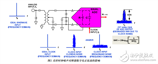
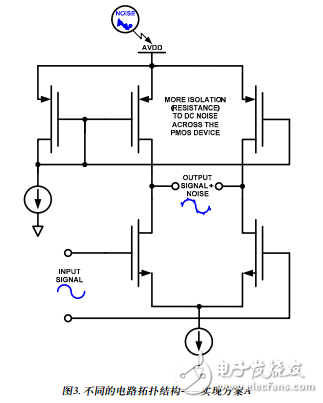
It can be inferred from this figure that it is a power supply pin. Replace the sample clock input pin in Figure 2 with an analog power supply pin (AVDD). The same principle applies here, ie any noise (near-carrier noise or broadband noise) will appear in the output spectrum in this convolution. However, there is one difference; the power supply pin can be thought of as a wideband input pin with a 40 dB to 60 dB attenuator depending on the process and circuit topology. In a general-purpose MOS circuit structure, any source or drain pin is essentially isolated (resistive) from the signal path, resulting in substantial attenuation, and the gate pin or signal path is not such. Assume that the design uses the correct circuit structure type to maximize isolation. In the case where the power supply noise is very obvious, some types (such as common source) may not be very suitable, because the power supply is biased by the resistive element, which is then connected to the output stage, as shown in Figure 3 and Figure 4 shows. Any modulation, noise, etc. on the AVDD pin may be more easily manifested, affecting local and/or adjacent circuits. This is why you need to understand and explore the PSRR data of the converter.
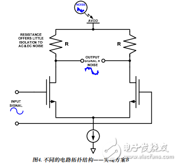
As shown in the different implementations, there are different frequency characteristics due to parasitic R, C, and mismatch. Remember, the process is getting smaller and smaller. As the process gets smaller, the available bandwidth increases and the available rate increases. With this in mind, this means lower power and smaller thresholds. For this reason, why not treat the power node as a high-bandwidth input, just like a sample clock or an analog input pin?
What is power suppression?
When there is noise on the power rail, there are three main factors that determine the performance of the ADC. They are PSRR-dc, PSRR-ac, and PSMR. PSRR-dc is the ratio of the change in supply voltage to the resulting change in ADC gain or offset error.
It can be expressed in fractions, percentages, or log-dB of the least significant bit (LSB) (PSR = 20 &TImes; log10 (PSRR)), usually with DC conditions.
However, this method only reveals how one of the ADC's nominal parameters may vary with the supply voltage, so the stability of the converter cannot be proven. A better approach is to apply an AC signal on top of the DC power supply and then test the power supply rejection (PSRR-ac) to actively couple the signal (noise source) through the converter circuit. This method essentially attenuates the converter and presents itself as spurs (noise) that rise above a converter's noise floor at a given amplitude. It is meant to indicate when the converter will collapse under the conditions given by the injected noise and amplitude. At the same time, this also allows the designer to understand how much power supply noise can affect the signal or be added to the signal. The PSMR affects the converter in different ways, which indicates the sensitivity of the converter to power supply noise when modulated with the applied analog input signal. This effect appears as a modulation applied to the converter near the IF frequency, which can severely damage the carrier sideband if the power supply is not designed to be rigorous.
In summary, the power supply noise should be tested and processed like any other input to the converter. The user must understand the system power supply noise, otherwise the power supply noise will increase the converter noise floor and limit the dynamic range of the entire system.
Power test
Figure 6 shows the settings for measuring the ADC PSRR on the system board. Each power supply is measured separately to better understand the dynamics of the ADC when an AC signal is applied across the power supply under test. Start with a high capacitance capacitor, such as a 100 μF non-polarized electrolytic capacitor. The inductor uses 1 mH, which acts as an AC blocker for the DC power supply. It is commonly referred to as the “bias-T†and can be purchased in a connector-packaged product.
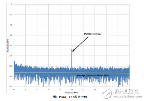
Using an oscilloscope to measure the amplitude of the ac signal, place an oscilloscope probe on the power supply pin of the ADC to be tested. For simplicity, the amount of AC signal applied to the power supply is defined as a value associated with the converter's full scale input. For example, if the full scale of the ADC is 2V pp, use 200 mV pp or –20 dB. Next, ground the input of the converter (without applying an analog signal) to find the error spurs at the test frequency in the noise floor/FFT spectrum, as shown in Figure 5. To calculate the PSRR, simply subtract –20 dB from the error spur value shown on the FFT spectrum. For example, if the error spur occurs at –80 dB of the noise floor, the PSRR is –80 dB – –20 dB, or –60 dB (PSRR = error spur (dB) – oscilloscope measurement (dB)). The value of –60 dB does not seem to be large, but if converted to voltage, it is equivalent to 1 mV/V (or 10−60/20), which is not very common for the PSRR specification in any converter data sheet. see.
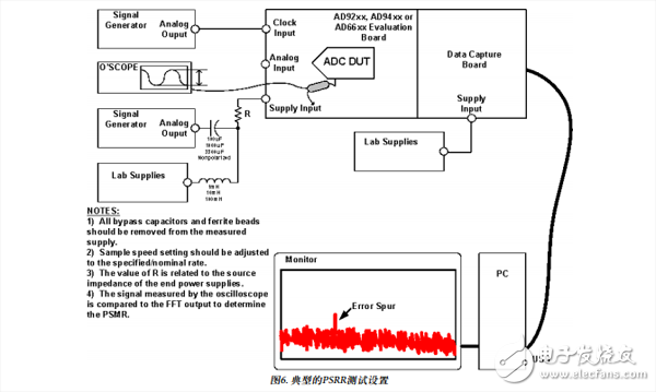
The next step is to change the frequency and amplitude of the AC signal to determine the PSRR characteristics of the ADC in the system board. Most of the values ​​in the data sheet are typical and may only be for the worst-case or worst-case power supplies. For example, a 5 V analog power supply may be the worst compared to other power supplies. Make sure that all power features are described. If the instructions are not comprehensive, please consult the factory. This way, the designer will be able to set the appropriate design constraints for each power supply. Keep in mind that there is a downside to testing PSRR/PSMR with LC configuration. When scanning the target band, the signal level required at the output of the waveform generator can be very high in order for the ADC supply pin to reach the desired input level. This is because the LC configuration forms a notch filter at a certain frequency that depends on the selected value. This greatly increases the ground current at the notch filter, which may enter the analog input. To solve this problem, simply swap in the new LC value when the test frequency is difficult to measure. It should also be noted here that the LC network also suffers losses under DC conditions. Remember to measure the DC power supply on the power pins of the ADC to compensate for this loss. For example, after a 5 V power supply passes through the LC network, there may be only 4.8 V on the system board. To compensate for this loss, simply raise the supply voltage.
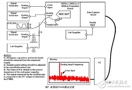
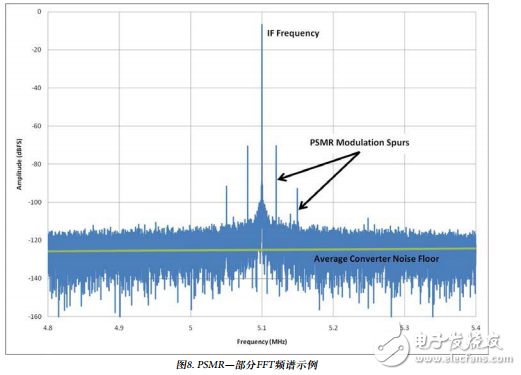
The PSMR is measured in the same way as the PSRR. However, when measuring PSMR, an analog input frequency is applied to the test setup, as shown in Figure 7. Another difference is that a modulation or error signal is applied only at low frequencies in order to see the mixing effect of this signal with the analog input frequency applied to the converter. For this type of test, a frequency of 1 kHz to 100 kHz is typically used. As long as the error signal, ie the mixing result, can be seen around the fundamental frequency, the amplitude of the error signal can be kept relatively constant. However, it is also possible to change the amplitude of the applied modulation error signal to check to ensure that the value is constant. To achieve the final result, the difference in amplitude between the highest (worst) modulation spurs relative to the fundamental frequency will determine the PSMR specification. Figure 8 shows an example of the measured PSMR FFT spectrum.
Power supply noise analysis
For converters and final systems, it must be ensured that noise on any given input does not affect performance. PSRR and PSMR have been introduced above and their significance. An example will be given to illustrate how to apply the measured values. This example will help the designer understand what aspects and how to design correctly in order to understand the power supply noise and meet system design requirements.
First, select the converter, then select the regulator, LDO, switching regulator, and so on. Not all regulators are suitable. You should review the noise and ripple specifications in the regulator data sheet, as well as the switching frequency (if using a switching regulator). A typical regulator may have 10 μV rms noise in a 100 kHz bandwidth. Assuming the noise is white noise, it is equivalent to a noise density of 31.6 nV rms/√Hz in the target band.
Then check the converter's power supply rejection indicator to see when the converter's performance will drop due to power supply noise. In the first Nyquist zone, fS/2, the PSRR of most high speed converters is typically 60 dB (1 mV/V). If the value is not given in the data sheet, please measure as described above or ask the manufacturer. A 16-bit ADC with a 2 V pp full-scale input range, 78 dB SNR, and 125 MSPS sampling rate has a noise floor of 11.26 nV rms. Noise from any source
The sound must be below this value in case it affects the converter. In the first Nyquist zone, the converter noise will be 89.02 μV rms (11.26 nV rms/√Hz) &TImes; √ (125 MHz/2). Although the regulator's noise (31.6 nv/√Hz) is more than twice that of the converter, the converter has a PSRR of 60 dB, which suppresses the noise of the switching regulator to 31.6 pV/√Hz (31.6 nV/√Hz). × 1 mV/V). This noise is much smaller than the noise floor of the converter, so the noise of the regulator does not degrade the performance of the converter.
Power supply filtering, grounding, and layout are equally important. Adding a 0.1 μF capacitor to the ADC supply pin can cause noise to be lower than the previously calculated value. Keep in mind that some power pins draw more current or are more sensitive than other power pins. Decoupling capacitors should be used with caution, but be aware that some power supply pins may require additional decoupling capacitors. Adding a simple LC filter to the power supply output also helps to reduce noise. However, when using a switching regulator, the cascaded filter can suppress noise to a lower level. It is important to remember that each additional level of gain increases by approximately 20 dB per 10 octaves.
One final point to note is that this analysis is only for a single converter. If the system involves multiple converters or channels, the noise analysis will be different. For example, ultrasound systems use a number of ADC channels that are digitally summed to increase dynamic range. Basically, for every doubling of the number of channels, the noise floor of the converter/system is reduced by 3 dB. For the above example, if two converters are used, the noise floor of the converter will become half (−3 dB); if four converters are used, the noise floor will become −6 dB. This is so because each converter can be treated as an uncorrelated noise source. The uncorrelated noise sources are independent of each other, so RSS (square root of the sum of squares) can be calculated. Eventually, as the number of channels increases, the noise floor of the system decreases, the system becomes more sensitive, and the design constraints on the power supply are more stringent.
in conclusion
It is impossible to eliminate all power supply noise in the application. No system can be completely immune to power supply noise. Therefore, as a user of the ADC, designers must be proactive in the power supply design and layout phase. Here are some helpful tips to help designers maximize the immunity of the PCB to power changes:
• Decouple all supply rails and bus voltages that reach the system board.
• Remember: each additional level of gain increases by approximately 20 dB per 10 octaves.
• If the power leads are long and supply power to a specific IC, device, and/or region, they should be decoupled again.
• Decouple both high and low frequencies.
• Series ferrite beads are often used at the power entry point before the decoupling capacitor is grounded. Do this for each supply voltage entering the system board, whether it is from an LDO or from a switching regulator.
• For added capacitors, use a closely stacked power and ground plane (pitch ≤ 4 mils) to provide high frequency decoupling capability in the PCB design itself.
• As with any good board layout, the power supply should be kept away from sensitive analog circuits such as the front-end stage of the ADC and the clock circuit.
• Good circuit segmentation is critical, and some components can be placed on the back of the PCB to enhance isolation.
• Note the ground return path, especially on the digital side, to ensure that digital transients do not return to the analog portion of the board. Separating the ground plane may also be useful in some cases.
• Keep analog and digital reference components at their respective levels. This conventional approach enhances isolation of noise and coupling interactions.
• Follow the IC manufacturer's recommendations; if the application notes or data sheets are not directly stated, the evaluation board should be studied. These are very good starting tools.
This technical article is intended to clarify the power sensitivity issues of high-speed converters and why it is so important to the user's system dynamic range. In order for the ADC on the system board to implement the performance specifications described in the data sheet, the designer should be aware of the required place-and-route technology and hardware.
Film Temperature Measurement Thermistor
Film temperature measurement NTC Thermistor is small and light as to be convenient to mounting. With the characteristics of high stability and reliability, superior electrical insulation and fast response, this type of thermistor can be used in household appliance, computer and printer etc.
Film Temperature Measurement Thermistor
Film Temperature Measurement Thermistor,Computer Sensors,Cpu Thermometer,Cpu Temp Monitor
Feyvan Electronics Technology Co., Ltd. , http://www.fv-cable-assembly.com