
Internet of Things applications spawn new smart foundries
It's hard to hear or see the discussion about IoT (Internet of Things) at an industry conference, but recently at the ICCAD Summit, a new foundry for IoT applications— - Triple Fujitsu Semiconductor is still making the Chinese IC industry shine! At this ICCAD summit, the newly established Triple Fujitsu Semiconductor Company and industry insiders discussed in depth how to meet the manufacturing needs of ICs or devices required for IoT applications. It is reported that Triple Fujitsu Semiconductor is a newly established professional foundry company that took over the 300mm production line and supporting equipment of Fujitsu Semiconductor in the Mie Plant in December 2014.
Accompanied by the great development of the Internet of Things
"With the rapid growth of the mobile communication market represented by smartphones/tablets, it is expected that the intelligentization of various fields such as automobile, medical and industrial, and the new market represented by IoT will grow and expand. The needs of enterprises will also start from the traditional miniaturization and other aspects of how to further reduce the power consumption of existing technology nodes." Mr. Hiroshi Hiroshi of Mitsubishi Semiconductor Business Development Department held the China in 2014 last month. The IC Design Industry Annual Conference and the China and Hong Kong Integrated Circuit Industry Collaborative Development Summit Forum (ICCAD Summit) said.
Figure 1. Mr. Hiroshi Hiroshi of Mitsubishi Semiconductor's Business Development Department.
In order to meet the design challenges brought by IoT and build a smart city in the future, Triple Fujitsu Semiconductor took over the 300mm production line and supporting equipment of Fujitsu Semiconductor in the Mie Plant in December 2014, and a professional OEM company came into being.
“As a foundry partner, we aim to help your business success through customized process skills and technical support. We are committed to meeting the needs of our customers through revolutionary solutions and rapid feedback. 'Becoming a smart society The new intelligent foundry is the goal of our efforts.†Mr. Waishan said.
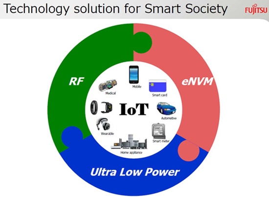
Figure 2. Triple Fujitsu Semiconductor's leading process solutions address IoT design challenges
The rapid growth of the wearable, mobile intelligence and IoT markets has brought new opportunities to the semiconductor industry, while Triple Fujitsu Semiconductor's outstanding technologies (ULP (ultra-low power technology), eNVM (non-volatile memory) and RF) Technical support (customized) will help customers achieve products that support the smart community.
Super CMOS technology (ULP, eNVM, RF)
"Reducing power consumption and controlling costs has become the biggest issue in the semiconductor industry. We will solve this problem by improving the most cost-effective planar CMOS process technology. This process technology is the key to the IoT market." Mr. Hiroshi Hiroshi said.
At the technical level, Triple Fujitsu Semiconductor has made process improvements based on basic CMOS processes, including: ULP (Ultra Low Power Technology), non-volatile memory and RF design.
1, ULP - the ultra-low power consumption required for mobile and wearable devices
As shown in Figure 3 below. To achieve the indispensable low power consumption of mobile wearable devices, Triple Fujitsu Semiconductor has developed the "C55ULP" processing technology. "C55ULP" has transistor and ultra-low leakage transistor technology that can operate at ultra-low voltages. In order to reduce power consumption, this transistor uses a different structure from conventional CMOS to achieve ultra-low power consumption. Therefore, when compared to the traditional 55nm CMOS technology, the "C55ULP" achieves a power reduction of approximately 50% compared to the "C55LP" at the same operating speed.
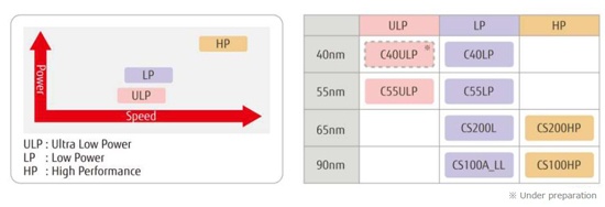
Figure 3. Using the same operating speed to reduce ULP technology by 50% compared to LP technology.
In addition, ultra-low leakage transistors also reduce leakage current from femtoamperes to picoamperes. "C55ULP" also offers a low-power solution tailored to the customer. “We are the first and only foundry company in the world to introduce ultra-low voltage and ultra-low leakage transistor technology and engage in mass production.†Mr. Waishan special emphasis.
2, eNVM - non-volatile memory that provides the lowest cost and high integration with CMOS
Non-volatile memory is widely used in various electronic instruments such as automobiles, IC cards, and smart meters. Triple Fujitsu Semiconductor will install a non-volatile memory with high integration with CMOS for customers at the lowest cost.
3, RF - to provide customers with the best RF solution
Wireless communication is also the key to the ever-changing IoT community. The Fujitsu Semiconductor's ULP/LP technology has the RF design required (variable diodes, inductors, MOM/MIM capacitors, etc.) and is equipped with PDK to provide customers with the best RF solution.
In addition, based on customer needs, Triple Fujitsu Semiconductor can customize its super CMOS technology in a flexible way, such as process optimization, parameter adjustment and so on.
“Our excellent CMOS technology will also provide flexible optimization process and parameter adjustment services according to customer requirements, and if the customer's products have been run in other foundry, we can also go to our factory for production, we will help to adjust the parameters. To reduce the difficulty of customer development.†Mr. Waishan pointed out.
Past life creates the future: rich IC manufacturing experience
Although Mie Fujitsu Semiconductor Co., Ltd. is the newly established company, it was not born out of thin air. Since Fujitsu Semiconductor took over the 300mm production line of the newly-launched Mie Plant in 2005, the company has commissioned the manufacture of advanced logic device LSI as its main business project. In October 2014, there were already 1,300 Tape outs. We will effectively utilize this rich experience and knowledge to provide customers with meticulous and prompt service from design to manufacturing.
In the future, Triple Fujitsu Semiconductor will also develop more high-performance solutions, as shown in the technical development roadmap shown in Figure 4.
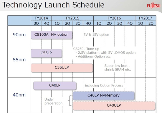
Figure 4. Triple Fujitsu Semiconductor Technology Development Roadmap.
And since the establishment of the Mie Plant, it has established a manufacturing system, information management, quality management and service customer system for the OEM business. In accordance with ISO14001, Mie Fujitsu Semiconductor has established an ISO9000 series and a quality assurance management system based on automotive ISO/TS16949 certification.
“The ability to produce automotive grade products is a big advantage for us. Not all fabs have the ability to produce automotive grade products. We will continue to make unremitting efforts to improve safety and product quality in the future.†Mr. Waishan stressed.
Postscript: Overview of Triple Fujitsu Semiconductor Corporation
The headquarters of Mie Fujitsu Semiconductor Co., Ltd. is located in Shin-Yokohama, Gangbuk-gu, Yokohama-shi, Kanagawa Prefecture, Japan. It is a high-tech industrial area in Japan, and many world-class technology companies are located here. “We have set up our headquarters and marketing base to expand our global business. The transportation is very convenient. Take the Shinkansen, which is about 1.5 hours from our factory in Kuwana City, Mie Prefecture.†Mr. Hiroshi Yamayama said.
In addition, in the earthquake response measures, the fab with a hybrid isolation structure in the semiconductor manufacturing industry, Triple Fujitsu Semiconductor is still the world's first. “We have installed three isolation devices between the building and the foundation to minimize the impact of microseisms under normal conditions to achieve a stable supply to customers.†Mr. Yuyama Hiroshi said.
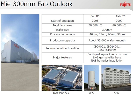
Figure 5. Overview of Triple Fujitsu Semiconductor Corporation
Now that everything is ready, Triple Fujitsu Semiconductor will rely on the strengths of ultra-low power process and memory embedded systems and equipped with experienced engineers, continuous improvement of production, based on high-risk response capabilities such as hybrid isolation buildings, and the world's most The favorite foundry company is striving to contribute to the technological innovation of the IoT society.
The Asus range of laptops is targeted towards the retail end-user market and hence the demand for the full range of Asus Laptop Charger is very high.
Asus laptop charger include Asus VivoBook charger series, ASUS Zenbook charger series, Transforme Book charger series and so on. If you want to find a replacement Power Adapter for Asus laptop, please feel free to contact us, we will help to select the correct OEM replacement Asus laptop Adapter for you.
The common Asus laptop charger specifications have 12V 3A 44W, 19V 1.75A 33W, 19V 2.37A 45W 19V 3.42A 65W, 19V 4.74A 90W etc, and the dc tip has 4.8*1.7mm, 4.0*1.35mm, 3.0*1.1mm, and special USB 6 pin, 40pin etc. Also Yidashun can produce 45W 5V/12V 2A 20V 2.25A type c adapter for Asus
Yidashun's laptop adapter is with smart IC to protect your laptop with over current protection, over load protection, short circuit protection, over heat protection. And all our Asus laptop adapter is Brand New Replacement Product, works as Genuine parts, 100% OEM Compatible!!


Asus Laptop Charger,Asus Charger,Asus Computer Charger,Asus Notebook PC Charger
Shenzhen Yidashun Technology Co., Ltd. , https://www.ydsadapter.com