
Application of AMBE-1000 Vocoder Chip in Voice Communication System
AMBE-1000 is a mature duplex vocoder chip developed by American DVSI and produced by Lucent. The chip uses AMBE speech coding algorithm, the coding rate is 2.4 ~ 9.6kb / s. AMBE (Advanced MulTI-Band ExcitaTIon) algorithm is an improvement and expansion of MBE (MulTI-Band ExcitaTIon) algorithm. The MBE speech coding algorithm divides the speech spectrum into several bands according to the pitch frequency, processes the unvoiced / voiced sounds (V, UV) of the signals of each band separately, and finally superimposes the signals of each band to form a full-band synthesized speech. The AMBE-1000 vocoder has better voice quality at low rate and strong background noise, which makes it widely used in mobile and shipborne mobile satellite voice communication systems. Inmarat (International Maritime Satellite Organization) has applied AMBE-1000 to its various generations of satellite voice communication systems. The chip can also be used in voice compression and storage systems. This article applies AMBE-1000 to the voice communication system, puts forward a specific implementation plan, and gives its telephone user interface loop, PCM voice digital coding loop and AMBE-1000 support circuit.
1 Introduction to AMBE-1000
1.1 Main features of AMBE-1000
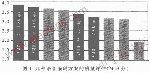
(1) Full-duplex encoder with high voice quality and low rate. The coding rate is variable from 2.4kb / s to 9.6kb / s. The comparison of voice quality with other vocoders is shown in Figure 1. Welcome to reprint, this article comes from the electronic enthusiast network (http: //)
As can be seen from Figure 1, at the coding rate of 4.8kb / s, AMBE-100 has very good voice quality; at the coding rate of 2.4kb / s, the voice produced by the chip is better than GSM voice.
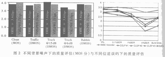
(2) Strong anti-background noise capability, FEC function, and good anti-channel interference capability, as shown in Figure 2.
It can be seen from Figure 2 that the AMBE-1000 algorithm's ability to resist background noise is significantly higher than that of other algorithms such as CELP.
(3) It has the advantages of low power consumption, and also has the functions of DTMF signal detection, identification, generation and transmission, as well as voice activation, comfort noise insertion and echo cancellation.
1.2 Basic working principle of AMBE-1000
The AMBE-1000 AD / DA voice interface signal can be a standard μ-law or A-law companded quantized PCM signal, or a 14- or 16-bit linear quantized PCM signal. The transmission interface of compressed voice data can be set to active or passive mode, and the data can be transmitted in serial or parallel mode. AMBE-1000 provides a series of pins used to set the default working state of the chip. When the chip is powered on, it automatically enters the default state set by the pins. These settings include AD / DA conversion format, voice encoding rate, FEC rate, active / passive mode, parallel / serial data mode, VAD enable, echo cancellation enable, etc. These states can be set by hardware, or can be changed by software through control words.
The data format of AMBE-1000 can be either a frame format or a non-frame format, usually using a frame format. For the frame format, AMBE-1000 works in full-duplex in parallel with a period of 20ms. After 20ms, AMBE-1000 compresses the digitized voice sent from the A / D converter, packs it according to its frame format and sends it to the coded output buffer, and decompresses and restores the data packet input from the decoder input buffer to D / A Converter to complete the encoding and decoding of digital voice.
2 Application of AMBE-1000 in voice communication system
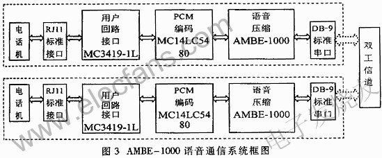
Based on the advantages of AMBE-1000, the overall block diagram of the system designed in this paper is shown in Figure 3. The system uses a telephone to input voice and provides a standard RJ11 interface. The interface circuit is implemented with MC3419-1L. The digital PCM coding of voice is realized by MC14LC5480, and finally AMBE-1000 is used to compress the voice.
2.1 User loop interface circuit
The subscriber loop interface circuit SCIL (Subscriber Loop Interface Circuit) mainly provides the "BORSHT" function for the subscriber telephone loop, which is realized by the MC3419-1L.
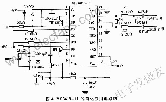
MC3419-1L is a user loop interface circuit interface chip produced by Motrola. Its basic performance includes: feeding DC power to the user loop; using current mirror, op amp and external balance network to complete 2/4 line conversion; with user line status Detection function, and output the corresponding level information. The current mirror is used in the MC3419-1L circuit to realize various main functions. The most important characteristic of the current mirror is that it can decompose an input current into several output currents, the input is low impedance, the output is high impedance, and the output input current has a strict proportional relationship. The MC3419-1L uses two of the six current mirrors to form a DC feed circuit. In order to improve the feeding ability and reduce the chip function, it is necessary to connect TIP125 / 111 as the power amplifier tube for output current; the chip's 2/4 wire transfer function is also implemented using op amps and current mirrors, and the second-line user loop signal (balanced signal) can be It is transmitted to the four-wire transmission output (unbalanced signal), and the signal of the four-wire reception input is not only transmitted to the user loop, but also through the balanced network to cancel the signal returned to the input of the transmission op amp to achieve the reception between the transmission Isolation; the user's on-hook and off-hook detection of the chip is also achieved through internal current mirror comparison.
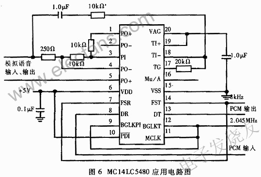
Figure 4 is a simplified application circuit of MC3419-1L. In Figure 4, TIP125 and TIP111 are current-fed power amplifier output tubes; the diode bridge and resistor between the -48 volt power supply and the user line mainly play the role of overvoltage and overcurrent protection, and the capacitor plays the role of anti-shock; access CC The external resistance-capacitance component of the foot is mainly used to suppress the common-frequency interference of power frequency; the connection part of MC3419-1L and PCM is a balanced network circuit.
2.2 PCM circuit
The PCM coding of voice is to convert analog voice signals into digital voice signals. It is the first step in speech digitization and the foundation of speech compression.
MC14LC5480 is a μ / A-law PCM chip produced by Motorola. It has the following characteristics: low power consumption; low-noise fully differential analog circuit design; on-chip integrated transmit band-pass filter and receive low-pass filter; with RC pre Filter after filter; μ / A law can be selected.
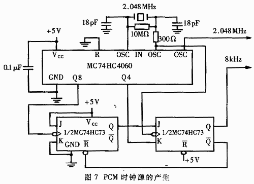
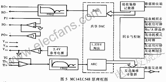
Figure 5 is a functional block diagram of MC14LC548.
In Figure 5, RO +, RO- and TI +, TI- are the differential output and input of PCM analog voice signal; PI, PO +, PO- are used to amplify the analog signal to drive the analog voice device; the synchronization control part is mainly used to control Frame synchronization and bit synchronization, the control pins are mainly used for μ / A law selection and low power consumption mode selection.
Figure 6 is the specific application circuit diagram of MC14LC5480.
In Figure 6, the 8kHz, 2.048MHz clock source can be generated by Motorola's MC74HC4060. The specific implementation is shown in Figure 7.
2.3 AMBE-1000 circuit
The circuit of AMBE-1000 is divided into three parts: interface with PCM; chip control pin setting; compression data input and output.
2.3.1 Interface circuit between AMBE-1000 and PCM
AMBE-1000 requires PCM voice data to be input and output in a serial manner. The key of this interface circuit lies in the frame synchronization and bit synchronization of PCM voice data. The specific implementation circuit is shown in Figure 8.
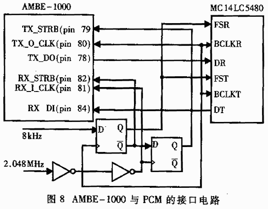
Among them, the input 8kHz clock source is used for bit synchronization, and the 2.048MHz clock source is used for frame synchronization. D flip-flop and inverter are used to synchronize the two clock sources.
2.3.2 Chip control pin settings
The pin setting of AMBE-1000 mainly includes the setting of the transmission interface, that is, the setting of the transmission interface mode for serial and parallel, active and passive, frame and non-frame, and also includes the setting of chip-specific functions.
The serial and parallel settings of the transmission interface is to select whether compressed voice data is input and output in 8-bit wide parallel mode or serial mode. The active and passive modes of the chip refer to whether the strobe signal for compressed voice data input and output is provided by AMBE-1000 or externally. The frame and non-frame modes mean that the input and output data are provided externally. Frame and non-frame mode refers to whether the input and output data are encapsulated in the AMBE-1000 fixed data frame format. In this system, AMBE-1000 is set to work in main, serial, and frame format.
AMBE-1000 specific function settings include AD / DA conversion format, voice encoding rate, FEC rate, VAD enable, CNI enable, echo enable, DTMF processing, and low power consumption mode. The pin settings set the default state that the chip automatically enters upon power-up. The above settings can also be changed through the software control word of AMBE-1000. The circuit of the pin setting can be realized by using a jumper seat and a jumper cap to facilitate the change of the hard setting.
2.3.3 Input and output circuits for compressed voice data
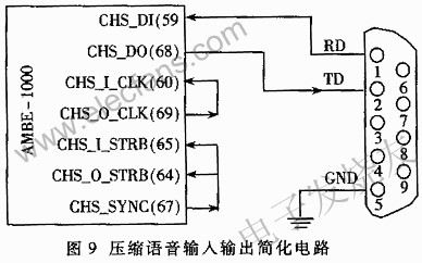
The input and output circuit of compressed voice data mainly refers to the setting circuit of the transmission interface and the connection circuit with the standard serial port DB-9. The transmission interface of this system is set to active, serial, frame format mode, that is, CH_SEL2, CH_SEL1, CH_SEL0 (98, 99, 2 pins) are set to 0, 1, 0. Figure 9 is a simplified connection circuit diagram of the chip and DB-9.
Among them, CHS_I_CLK (serial input clock), CHS_O_CLK (serial output clock), CHS_I_STRB (input data strobe), CHS _) _ STRB (output data strobe), and CHS_SYNC (serial synchronization) in AMBE-1000 are used for input and output Clock synchronization. Welcome to reprint, this article comes from the electronic enthusiast network (http: //)
LED Flood Light made by aluminum alloy. Surface coating by special technology or anodizing aluminum process, impact resistant,sturdy and durable features. Fins design of heat,rational utilization cross-ventilation to improve products stability and working life.
SMD LED Flood Light, the Waterproof level of LED Flood Light is IP65.IP66.IP67.All of them applied in commercial and residential.
LED Flood Light
LED Flood Light,High Power LED Floodlight,LED Outdoor Flood Lighting,Explosion Proof LED Flood Light
Wenzhou Korlen Electric Appliances Co., Ltd. , https://www.korlenelectric.com