
Design and Implementation of Optical Wireless Communication System Based on Ethernet
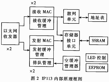
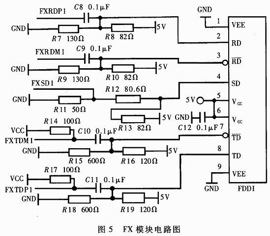
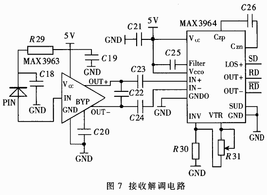
Abstract: An optical wireless communication system based on Ethernet is introduced. The system uses the high-performance Ethernet transceiver chip IP113 as the core, with the necessary peripheral devices, combined with the modulation drive circuit and the receiving and demodulating circuit developed, to realize the system design of Ethernet for long-distance communication by light waves. Keywords: Ethernet IP113 PECL The history of optical communication using light waves as an information carrier has a long history. Atmospheric laser communication is communication using the atmosphere as a transmission medium. It is the first communication method developed after the advent of lasers. Because it has the advantages of long transmission distance, frequency bandwidth, small transmitting antenna, good confidentiality and anti-electromagnetic interference, etc., it has attracted more and more attention, and its application has become increasingly widespread. Ethernet is the most widely used networking technology. It is widely used in enterprises, schools and other fields due to its high reliability, large amount of media information, and easy expansion and update. According to IEEE 802.3 Ethernet standard, the length of each coaxial cable of Ethernet should not exceed 500m. After interconnecting through repeaters, the maximum distance of the network should not exceed 2.8km. In this case, the use of laser wireless communication technology, beyond the geographical limitations of Ethernet, to meet the needs of data communication, has a strong application value. Combining Ethernet and laser wireless communication to give full play to the advantages of the two can greatly improve the application range and reliability of the system. Figure 1 is a schematic block diagram of one end of an Ethernet-based laser wireless communication system. The structure at the other end is symmetrical to the local end. Bipolar MLT-3 data signal from the computer network card, The Ethernet transceiver circuit is composed of RJ45 interface, coupling transformer, Ethernet transceiver, and the interface between the transceiver and the modulation drive circuit and receiving demodulation circuit. The Ethernet transceiver is the core unit, which directly determines the performance of the system. 2.1 Ethernet transceiver IP113 This system uses the Ethernet to fiber transceiver IP113 chip produced by IC PLUS. IP113 is a two-port (including TP port and FX port) 10 / 100Mbps Ethernet integrated switch, consisting of a two-port switching controller and two Ethernet fast transceivers. Each transceiver complies with IEEE 802.3, IEEE 802.3μ, IEEE 802.3x rules. SRAM is reserved for the frame buffer, which can store a 1K byte MAC address, full digital adaptive adjustment and timing recovery, baseline drift correction, and full / half duplex working at 10 / 100baseTX and 100baseFX. Use 2.5V single power supply, 25MHz single clock source, 0.25μm technology, 128 pin PQFP package. 2.2 Ethernet transceiver circuit design The Ethernet transceiver circuit is shown in Figure 3. It is mainly composed of the Ethernet transceiver chip IP113, the dedicated configuration chip EEPROM 93C46, the LED display matrix, and the interface between Port1 and TP module of IP113, Port2 and FX module. When resetting, IP113 first reads the content of 00H of 93C46. Only when 00H [15: 0] = 55AA, it will continue to read the parameters from EEPROM, otherwise it will work with default value or specific pin level setting. register. The value in 01H sets the LED output control register to control the on, off, and blinking of the two LED matrices to show the connection, activity, full / half duplex, and rate (10 Mbps / 100 Mbps) of the two ports, respectively. The value in 02H sets the exchange control register 1, which selects the system's flow control mode and conflict protection. The value in 03H sets the exchange control register 2 to control packet loss, address failure, priority and algorithm compensation of the system. The value in 04H sets the transceiver control register, among which the five values ​​of 04H [13:11]: 00, 100, 101, 110, and 111, respectively correspond to the five working states of the transceiver: NWAY, 10Mbps (half-duplex) ), 10Mbps (full, half duplex), 100Mbps (half duplex) and 100Mbps (full, half duplex). The values ​​in 05H ~ 0AH set the transceiver confirmation register, test register and verification mode register respectively. Port 2's FXRDP and FXRDM are the receiving data pairs of FX, and FXTDDP and FXTDDM are the transmitting data pairs of FX. FXSD is a photoelectric detection signal. When the level of the received optical signal after photoelectric conversion is lower than 1.2V, FXSD outputs a continuous PECL level. Figure 5 is the circuit diagram of the FX module, using a standard FDDI data interface in the circuit. Because the 5V power supply is used for the modulation driving and receiving and demodulation circuits, and 2.5V power supply is used for the other parts of the system, the signals in FDDI are all PECL levels, so they must undergo level conversion (as shown in Figure 5) to convert this The two parts are connected. 3 Modulation drive circuit design Fig. 6 is the modulation drive circuit diagram, which is mainly composed of the MAX3253 chip of MAXIM's 155MHz and the laser LD with monitor diode inside. The main bias power supply inside MAX3263 provides temperature-compensated bias and reference voltage outputs Vref1 and Vref2. The internal high-speed modulation drive circuit, laser, and monitor diode are programmed through resistors R25, R26, R27, and R28. The output current of MAX32263 is controlled by the internal mirror current source. These mirror current sources all have a junction temperature drift of 2Vbe. When the reference voltage is set at 2Vbe, the junction temperature drift can be offset. Resistor R28 is selected to adjust the laser static bias current Ibo, so that Ibo is slightly less than the threshold current of the laser, so that the output of the laser has a good extinction ratio. The monitor diode inside the LD converts the light intensity change into a current Ipin, which generates a feedback current Ibs through internal conversion. The light intensity change of the laser is converted into a part of the bias current by the formula Ibo = 40 (Ib + Ibs), and the feedback acts on the laser Ensure stable output of optical power. The input differential PECL signals RD and RD are modulated by a modulator composed of an internal high-speed input buffer and a common emitter differential output. The magnitude of the modulation current is determined by the current Im determined by R26. Choose the size of R26 so that the laser has an appropriate modulation current, output enough optical power, and have a good extinction ratio. At the same time, the voltage at OUT + and OUT- should be above 2.2V to prevent laser saturation. Figure 7 is the receiving demodulation circuit diagram, which is composed of MAX3963 and MAX3964 with necessary peripheral devices. The 155MHz low-noise chip MAX3963 constitutes a preamplifier, which contains a transimpedance preamplifier and an inverting amplifier with emitter follower output, and integrates a 22kΩ transimpedance, which can convert the weak photocurrent received by the PIN into Differential output voltage. The MAX3964 of 266MHz constitutes the post-amplification conditioning circuit. There is a serial power detector composed of 4 limiting amplifiers inside, and each limiting amplifier has a full-wave logarithmic detector to detect the power of the input signal. The four test results are added together at the Filter terminal and filtered by the capacitor C25. Resistors R30, R31, the internal 1.2V reference power supply and the non-lighted comparator together constitute the threshold setting and noise suppression functions. Take R30 = 100kΩ, R31 can be adjusted with a potentiometer of 100kΩ, then VTR changes between 1.2 ~ 2.4V. When the input signal amplitude is greater than VTR, output a stable PECL level signal; when the input signal amplitude is less than VTR, the data output terminal OUT + output high level, OUT-output low level, all limiting amplifiers refuse to accept input Signal, and the post-stage amplifier outputs a light-free alarm PECL signal los +. 5 System test On the basis of the designed parts, they are connected, and the experiment of indoor Ethernet laser wireless communication is successfully carried out without the optical antenna. The system is now being perfected and is ready to be applied to optical networks. |
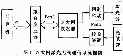
 Through the RJ45 interface, after passing through the coupling transformer, it becomes a unipolar level signal and sent to the Ethernet transceiver. The high-speed PECL signal generated by the modulation drive circuit directly modulates the intensity of the laser to drive the laser to emit light. The optical antenna is emitted. The receiving optical antenna converges the laser signal reception on the photosensitive tube. After receiving the demodulation circuit, the PECL high-speed data signal is recovered, and then sent to the computer through the coupling transformer to complete the entire communication process. As can be seen from Figure 1, the system is mainly composed of three parts: Ethernet transceiver, modulation drive circuit and receiving demodulation circuit. The circuit design of these three parts will be explained in detail below.
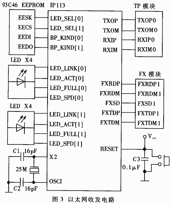
40152 17Ah 3.2V Lithium Ion Battery
Lithium Solar Batteries,Panasonic Lithium Ion Battery,Hw40152L 17Ah Lifepo4 Battery,Hw40152S 17Ah Lifepo4 Battery
Zhejiang Xinghai Energy Technology Co.,Ltd , https://www.headwayli-battery.com