
Design detailed tutorials for band-blocked frequency selective surfaces
The frequency selective surface (FSS) is a two-dimensional periodic array structure consisting of periodically arranged metal patch elements or aperture elements periodically arranged on a metal screen. Such surfaces can exhibit total reflection (patch type) or full transmission (aperture type) near the unit resonance frequency, which are called band-stop or band-pass FSS, respectively. The actual tape blocking section consists of one or more layers of FSS patches separated by a dielectric layer. For the stability of the FSS frequency response with respect to the incident angle and polarization, the metal patch layer is usually embedded in the multilayer dielectric layer. In addition, the back-to-back stacking of two or more layers of FSS patches results in very good passband characteristics (flat passbands, steep drop sidebands).
2 Design of band-rejection frequency selection surface A typical bandstop filter consists of two FSS metal layers and an intermediate dielectric layer. The middle dielectric sheet determines the flatness of the transmission curve passband, and the FSS metal layer determines the bandwidth and resonant frequency of the transmission curve. The thickness and dielectric constant of the dielectric sheet are very important. The thickness of the dielectric sheet is typically taken at 0.5  , It is the wavelength of the center of the stop band. The dielectric layer between the two FSS layers improves the stability of the bandstop filter with respect to the incident angle. Although from the standpoint of stability, the higher the value of the dielectric coefficient is, the better, but the high value also introduces a high transmission loss. In this way, according to design requirements, comprehensive consideration must be given to the value of the dielectric coefficient.
The goal of this paper is to design a signal that the FSS structure can pass the signal in the GPS & DCS1800 mobile communications band and reject the higher frequency band. Figure 1 shows the geometry and configuration of the designed frequency selective surface.
It consists of two FSS layers separated by a foam gasket. The circular ring-shaped cell block shape was chosen because of its good frequency band stability. The FSS metal layer is embedded in the dielectric constant  For a 3.5 polyimide layer with a loss factor of 0.0026. Thickness of foam gasket is taken close to 0.5
  =
=  , where the resonant frequency of the FSS is
  ,
,  . The design of this bandstop filter will be analyzed using the Smith chart and transmission line theory.
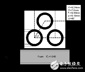
Figure 1 Two-layer circular FSS structure
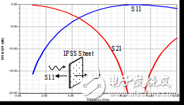
3 Analysis and design with Smith chart and transmission line theory The design starts with a layer of FSS consisting of a circular FSS metal layer embedded in a dielectric layer. The dielectric layer has a dielectric constant of 3.5 and a dissipation factor of 0.0026. The structure is analyzed and designed by simulation software Ansoft DesignerTM. Figure 2(a) shows the impedance of a layer of FSS on the frequency band from 1GHz to 12GHz. The corresponding transmission and reflection frequency response is  with
with  Shown in Figure 2(b). A layer of FSS transmission line equivalent circuit and the corresponding formula are shown in Figure 2(c). For comparison, the five points in Figure 2(a) are marked to represent the passband at 1GHz, 2GHz and the stopbands at 5GHz, 7GHz, and 9GHz, respectively. Observable admittance trajectory
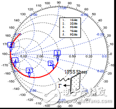
Fig. 2(a) Admittance track of a layer of FSS
(b)
Figure 2(b) One layer of FSS  with
with 
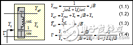
Figure 2(c) Equivalent Circuit and Formula for a FSS Transmission Line
In the circle where the conductance is equal to 1, it is implied that the real part of the quadratic admittance is equal to the admittance of air (that is,  =1/377 mhos), which can also be obtained from equations (1.2) and (1.3). From Fig. 2(a), it can be observed that the reflection coefficient is 9GHz.
  , and in Figure 2(b) at 9GHz
  It is consistent.
Figure 3 shows the results of an additional layer of 25.4 mm thick spacers added to a layer of FSS structure. Comparing Fig. 3(a) with Fig. 2(a), we can see that there is only a small change at 1 GHz and a rotation of 1200 at the 2 GHz admittance value. This can be explained by equation (2.2). The frequency changes to the edge of the admittance diagram at the 7 GHz and 9 GHz points. It implies a high reflection coefficient at these frequencies, which can also be seen in Figure 3(b). The second layer of FSS was added to the shims and the results are shown in FIG. As can be seen from Figure 4, the high frequencies are concentrated on the left side of the admittance graph, and most of the frequency points are concentrated on the edge of the table, which means that the reflection band is widened with the addition of the second layer FSS.
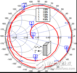
Fig. 3(a) Admittance trajectory of a layer of FSS plus a layer of spacers
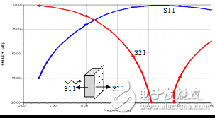
Figure 3(b) One layer of FSS plus one layer of spacer s11 and s21
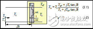
Figure 3(c) Equivalent circuit of transmission line with one layer of FSS and one layer of spacer
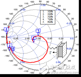
Figure 4(a) Admittance trajectory of two-layer FSS plus one-layer spacer
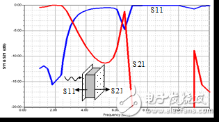
Figure 4(b) Two-layer FSS plus a shim s11 and s21
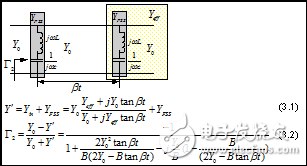
Figure 4(c) Equivalent Circuit of Transmission Line with Two Layers of FSS and One Layer of Gasket
4 ConclusionThe goal of this paper is to design a band-stop FSS structure that allows the rejection of higher frequency signals through the GPS & DCS1800 signals. The two-layer FSS, the structure separated by the foam spacer in the middle, was guided and the frequency response was simulated by simulation software. The FSS structure gives an analysis of the Smith chart and transmission line theory.
Crystal Clear Back Sticker,Phone Sticker,Mobile Phone Back Skin,Crystal Clear Phone Skin
Shenzhen Jianjiantong Technology Co., Ltd. , https://www.jjtscreenprotector.com