Talk about the typical DDC and DUC integrated in the IF/RF converter
To meet the ever-increasing data demands of smartphones, the infrastructure of modern digital mobile communication systems must continue to evolve to support wider bandwidth and faster data conversion. In order to achieve high speed data rates, digital intermediate frequency processing in digital converters, including DDC (Digital Downconverter) and DUC (Digital Upconverter) are the main functional modules.
These digital functions can be implemented in DSPs and FPGAs, and some large companies will build their own digital IF processing ASICs. Analog Devices is integrating more and more of these digital IF processing blocks into high-speed converter ICs, dramatically reducing design effort and saving system cost and power. This article explores the integrated DDC and DUC channels in ADI's IF and RF converters and shows how they work in real-world applications.
High-speed converters are one of the key functions of modern wireless base station systems. More and more such converters integrate complex digital signal processing blocks to simplify FPGA operation in system design. The digital signal processing module in the converter is very beneficial to the system design, but these benefits have not been fully understood by many engineers. It is hoped that this article will provide a clear description of the DDC and DUC functions in the data converter, allowing system designers to take full advantage of the benefits of the ADI converter to the transceiver architecture. Note: This article will focus on digital processing blocks in ADCs and DACs; therefore, in some descriptions the transmitter and receiver modules are combined. Please ignore signal flow that may cause confusion.
In modern digital mobile communication systems, the transmit and receive paths (including the feedback receive path in the description below) can be divided into three main circuit levels depending on the signal characteristics: the radio frequency level, the analog intermediate frequency level, and the digital intermediate frequency level. Figure 1 is a block diagram of a typical transmitter and receiver. The RF stage processes RF signals. In the current LTE standard, the signal frequency range is typically 700 MHz to 3.8 GHz.
After being processed by a mixer, modulator, or demodulator—all of which are mixing units—the RF signal moves to a lower frequency below DC to 300 MHz. The processing module from the data converter to the mixer includes a converter (ADC or DAC), an analog filter, and an intermediate frequency amplifier. We can call this level the analog IF level.
After the converter (actually after the quantizer portion of the converter), the signal becomes a digital signal; it is combined with the subsequent FPGA or ASIC, which we call the digital intermediate frequency stage. For each digital signal processing module in this stage, it is commonly referred to as DUC (Digital Upconverter) in the Tx path and as DDC (Digital Downconverter) in the Rx path.
The exception is the direct RF architecture, where the data converter samples the RF signal directly, so there is no analog IF stage, and the signal chain consists only of the RF stage and the digital IF stage.
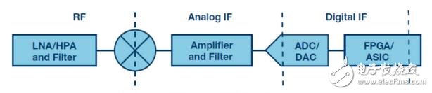
Figure 1. Typical block diagram of a transmitter or receiver.
A typical DDC module includes carrier selection, downconverter, filter, and decimator. These functional blocks operate in sequence, or can be bypassed separately, resulting in a complex signal or a real signal at DC, depending on the requirements of the subsequent FPGA or ASIC (which has a lower sampling rate).
Typical DUC modules include interpolation, filters, upconverters, and carrier combiners. Depending on the system architecture design, the DUC generates a complex or intermediate frequency signal at DC or directly generates a RF signal. The processing of the DUC is almost the opposite of the processing of the DDC.
Multiple DDC and DUC levels are often cascaded to provide flexibility. Independent DDCs and DUCs need to process multiple carriers in parallel, outputting the transmitted signals after combining or separating them in the received signal.
DDCThe Rx link requires a higher sampling rate to avoid signal aliasing, simplifies the analog filter design, and provides a wider signal band. On the other hand, to save power, cost, and high-speed logic in FPGA/ASIC, it is best to reduce the data rate on the interface. The integrated DDC of the converter will address the above requirements. Figure 2 is a block diagram of a typical DDC.
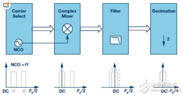
Figure 2. DDC block diagram
NCO and mixerTo select the desired carrier from the interference (blocking signal and other carriers), the output frequency of the NCO is mixed with the input IF signal to shift the desired carrier frequency to DC. This reduces the complexity of subsequent filtering and decimation stages.
Filtering and extractionAfter the NCO and mixing stages, a low pass filter is used to select the desired filtering and reject other unwanted signals. After the filter, a 2x extractor is used to reduce the data rate. To save resources and provide flexibility to the customer, the half-band FIR filter plus 2x extractor is combined in one module; the module is reused to cascade three to four levels. The system designer can choose to use some or all of them depending on the application needs. The converter may also provide other decimation rates beyond 2x to provide greater flexibility, especially in RF ADCs.
DUCThe Tx chain has the same requirements as the Rx chain: a high sampling rate is required to simplify the filter design, the signal frequency is at a high intermediate frequency or directly into a radio frequency, and the image is pushed far away, but the interface expects to use a lower data rate. The integrated DUC of the converter will address these requirements. Figure 3 is a block diagram of a typical DUC.
Interpolation and filtering
The simplest digital interpolation algorithm is called "zero padding", which inserts 0 between every two samples. The sampling rate is doubled, but a mirror with a frequency of Fs –Fif is also generated in the resulting spectrum. Therefore, a filter stage is required after the interpolator to eliminate the mirror or raw carrier (depending on the application). If the original carrier is eliminated, the result will be the coarse adjustment of the interpolation and Fs/2.
As in the DDC, 2x interpolation and filters are combined into one module. Then repeat this function module and cascade three to four levels to increase flexibility. Other interpolation coefficients other than 2x can also be used to provide greater flexibility, especially in RF DACs.
NCO and mixerThe NCO and mixer stages in the DUC are very similar to the same modules in the DDC, but with the opposite function, that is, the carrier frequency is shifted to the desired intermediate or RF frequency according to the requirements of the system architecture. In a zero-IF architecture, this module can be bypassed to keep the carrier at DC.
Gain, phase, I/Q offset, and inverse Sinc
Gain, phase adjustment, I/Q offset, and anti-sinc modules are add-ons to many IF/RF DACs.
Gain, phase adjustment, and I/Q offset are often used together to independently tune the output signal I/Q channel to compensate for different types of I/Q mismatch (caused by DAC, analog filter, and modulator), ultimately from the analog modulator Outputs an ideal complex signal with low LO leakage and low mirroring.
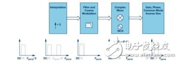
Figure 3. DUC block diagram
The inverse sinc filter compensates for the sinc roll-off caused by the DAC, which affects flatness and signal amplitude, especially in broadband applications with high IF or direct RF architectures.
to sum up
This article briefly describes the typical DDCs and DUCs that are currently integrated in IF/RF converters - what they are, why they are needed, and how they work in the signal chain. Proper understanding of these and proper use of them will reduce resource consumption and ease coding in FBGA/ASIC, as well as save system power and cost.
KNB1-32 Miniature Circuit Breaker
KNB1-32 Mini Circuit breakers, also named as the air switch which have a short for arc extinguishing device. It is a switch role, and also is a automatic protection of low-voltage electrical distribution. Its role is equivalent to the combination of switch. Fuse. Thermal Relay and other electrical components. It mainly used for short circuit and overload protection. Generally, According to the poles, mini Circuit breaker can be divided into 1P , 1P+N , 2P, 3P and 4P.
KNB1-32 Miniature Circuit Breaker,KNB1-32 Electronics Miniature Circuits Breaker,KNB1-32 Automatic Miniature Circuit Breaker,KNB1-32 Mini Circuit Breaker
Wenzhou Korlen Electric Appliances Co., Ltd. , https://www.zjmotorstarter.com