
This is a plus 3T National Bank passport according to the 128GB version to sell to 3K?
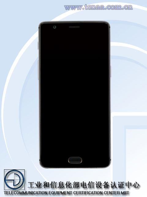
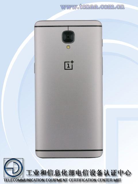
Tencent digital news (water blue) the latest release of one plus 3T will be officially debut on November 29 in the country, and the state bank version of the aircraft has also got a network license, and the Ministry of Industry and Information Technology announced the "certificate photos", Compared with one plus three in terms of appearance, it has not changed, but in the past, the gun-gray version was added on the basis of glacier ash and mint gold, and it supports the B5 and B8 bands of FDD-LTE network. It is expected to be sold in 128GB version. The price may be 2999 yuan.

Passport exposure
According to the latest information released by the Ministry of Industry and Information Technology, a new aircraft with its model number A3010 has obtained a network access permit. If it is unexpected, it should be a one-plus-three-nation T-country version released at the end of the month. According to the ID photos released by the Ministry of Industry and Information Technology, the appearance of the aircraft did not change from the one plus three, but in the past, the gun-gray version was added to the glacier ash and mint gold.
In addition, one plus 3T BNM also increased support for B5 and B8 bands in FDD-LTE networks, but in the parameters announced by the Ministry of Industry and Information Technology, the rated capacity of the batteries used by the aircraft is still 3,000 mAh. This is not the official 3,400 mAh previously announced. In addition, one plus A3010 has also obtained 3C certification, and the matching charger model is different from one plus three, although the output power is still 5V/4A, but it is said that the charging speed exceeds Google Pixel XL, and even the official also Gives the idea of ​​charging half an hour and cruising for a whole day.
There will be four major upgrades
As a follow-up upgrade of one plus three mobile phones, one plus 3T has four major upgrades in the past. First of all, although the main camera of the aircraft maintains its original specifications, sapphire glass has been added to protect the lens, and optical image stabilization and video recording have also been improved. Secondly, one processor with 3T is upgraded from Snapdragon 820 in the past to Snapdragon 821 processor, and the main frequency speed reaches 2.35GHz. In addition, the aircraft also has 6GB of memory, but an increase of 128GB capacity version.
One Plus 3T also upgraded the front lens from the previous 8 million pixels to 16 million pixels, and switched to the Samsung 3P8SP sensor. The single pixel area is 1.0 micron, the lens aperture is still F2.0, and the detection phase focus is supported. Record 1080p video pictures in 30fps format. However, according to the parameters announced by the Ministry of Industry and Information Technology, the Bank of China version seems to be only available in 128GB versions.
Or sell 2999 yuan
In addition to hardware upgrades, one plus 3T has also been optimized on the system UI, adding new features such as finger-sliding screenshots, designated password protection, and quick access to contacts under the lock screen. At the same time as a Canadian official said on Twitter that the underlying source code has been announced, so plus 3T is still in the near future "Brush Prince".
As for the price that everyone is concerned about, according to sources from Yijia Community, the price of a 64GB version with a 3T national bank may be 2799 yuan, while the 128GB version may be set at 2999 yuan. Of course, the premise is that one plus 3T has a 64GB capacity version in China. At present, the price of one plus 3T Hong Kong version has been announced, and the selling price is starting from 3388 Hong Kong dollars, which is approximately 3,000 yuan, but it is unclear when the specific sale time.
Via in Pad PCB
What is Via in Pad? In shortly,via in pad is the via holes are at the SMD pad.The vias are very small,usually under 0.3mm.Why and how? First is there is no enough space to layout,you have to put the vias and holes closer even together.Second it helps thermal management and for high frequency boards,it may help improve signals.
Because the SMD pads are for SMD components loading,so the solder can not flow to inner layer or the other side when assemble.That is the most important for via in pad board.
How PCB manufacturers like us to do via in pad board? We will fill all vias with non-conductive epoxy and plate copper over it ,so the vias are flat same as others. Many PCB factories are unable to do such capability.
The key technology is how we fill vias and guarantee there is no any solder (surface finishing) in the holes.
Filled via in pad is a way to achieve intermediate density with an intermediate cost compared to using blind/buried vias. Some of the key advantages associated with using the via in pad technology are:
.Fan out fine pitch (less than .75mm) BGAs
.Meets closely packed placement requirements
.Better thermal management
.Overcomes high speed design issues and constraints i.e. low inductance
.No via plugging is required at component locations
.Provides a flat, coplanar surface for component attachment
Via in big pads are not a big problem.but for BGA,that is technology.As BGA pads are very small,10mil or 12mil,and there is no enough space.Manufacturing is not easy as other boards.
Via In Pad PCB,6Layer Via In Pad PCB,Touch Pad PCB,Via In Pad
Storm Circuit Technology Ltd , https://www.stormpcb.com