
FPGA in 2032: ACM FPGA 2012 Annual Seminar
Beginning this year, the 20th FPGA International Symposium of the Computer Society (ACM) will hold a future discussion: What will FPGAs look like in 20 years? Experts from suppliers, users, and academic communities will participate in this event to make deterministic final predictions for the future.
By summarizing the best projects, the seven speakers will review the history of programmable devices over the past 20 years, summarizing the trend lines, and based on this, deductive. Experts will sketch the future of FPGAs in three main areas: process technology, architecture, and metaphors and tools for programming devices.
Process technology
The development of microelectronics over the past two decades will outline the future of FPGAs. Speakers generally believe that by 2032, the main factor driving this development is undoubtedly the evolution of CMOS scale.
Ivo Bolsens, Xilinx CTO and Senior Vice President, believes: "The development of silicon wafers will continue for 25 or 30 years. Before 2030, I don't think there will be new materials in this area."
Misha Burich, senior vice president of CTO and R&D at Altera, presented the topic of the discussion. He has a similar view. From quantum transistors to DNA, there are many attractive technologies, but he does not intend to discuss it in depth. He continued to make comments that Altera's process development will continue until 2026. Burich commented: "Since then, Moore's Law can still be used as a standard."
So what does Moore's Law reveal? Burich believes: "In 2032, we will introduce a 1.8-nm process with a 3-nm feature size and metal-1 pitch. This means we can achieve 878 billion transistors on a single die." Burich expects this type of FPGA to be 250 times faster than today's devices. However, the CTO reminded that for silicon wafers, there are only 13 atomic intervals at 3 nm. Even with atomic process control technology, compared to the tolerances of many current circuit designs, a simple quantization example, a 12-atom long channel and a 14-atom long channel, will have a large transistor. The change. Although smaller transistors will be faster, the interconnect will be very slow and will require a re-examination of the traditional view of circuit topologies. In fact, this requires a breakthrough in cell-based design.
Peter Cheung, head of the Department of Electrical and Electronic Engineering at the Royal College of London, elaborated on some of the practical dilemmas facing this issue. Cheung predicts: "If you want to design a chip that works with every transistor in 2032, then your output is zero. In fact, process changes will make each chip physically unique. And, at the end of the manufacturing process, this difference will still exist."
Cheung reminded: "This brings problems. We already know that over time, many mechanisms, including defective charges, hot carrier effects, impedance enhancement, and ion diffusion, can significantly degrade the circuit. The effect of the current effect on the work of the chip is not obvious, but it will become more and more obvious in 20 years."
To some extent, Cheung sees this as an opportunity for programmable logic. He suggested that programmable devices are not just a way to implement a system. In 2032, every system-level device is programmable: at runtime, the chip configures its still-operating resources into the working system. Cheung commented: "In view of this, we believe there are new opportunities for reconfigurability. They include device-specific fine-tuning; self-test, characterization and diagnostics; failure prediction; reconfiguration, recovery from failure; avoiding worst The design in the case; and the loss equalization over time, which extends the life of the chip."
Several speakers also introduced other key process scale issues: off-chip I/O bandwidth has not increased with the internal performance of the chip. Bolsens believes: "3D applications will solve the interconnect bandwidth problem to some extent. However, 3D itself will bring new problems. We will see that 2.5D is more and more complex, including passive and interpolated memory, etc. On the fast 2.5D will not disappear quickly. It still takes more than ten years for the full 3D to mature."
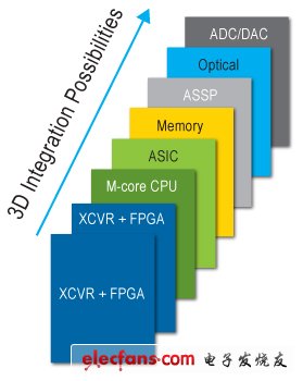
The more conservative Burich warns that in addition to technical issues, 3D faces many business relationship issues. He warned: "It may take more than ten years to resolve these issues."
Architecture
Over the years, process technology and application requirements have driven substantial changes in the FPGA architecture. Previously, the process was only focused on the number of small transistors, and the application focused on glue logic. The FPGA conference had a heated debate on whether heterogeneous devices were superior to homogeneous logic cells. Today, the debate in this area seems to be over, but the speaker pointed out that this is not the case.
Burich pointed out: "Today, only 40% of FPGAs are logical architectures." He explained that the rest of the die includes RAM, arithmetic hardware, I/O, high-speed transistors, protocol engines, and sometimes CPU cores and buses. And some support circuits, etc. Burich claims: "By 2032, all chips are heterogeneous." In fact, he believes that large-scale IC architectures are convergent. In the end, all seem to be dedicated chip systems (SoCs), and some chips can be partially reconfigured with substantial differences.
Although the heterogeneous architecture is very successful, there is one notable exception. Bob Blainey, a Distinguished Research Fellow in IBM's Compilation and Next-Generation System Software, said that his world is server computing, not silicon. He described the future as most servers are built into a vertical 3D IC die stack. The server itself is just a stack of dies, and it also includes local memory, interconnects, and large-scale homogeneous FPGAs.
Blainey explained that such FPGAs will become virtual resources for servers: a protected virtual architecture in which system software can dynamically build shareable accelerators. These devices actually incorporate a large number of dynamically reconfigurable logic gates that are managed by a hardware-based hypervisor that controls the creation, teardown, sharing, and security of logic gates.
There are subtleties between these two completely different architectures. In general, designers considering SoC replacement, such as designers in the field of mobile devices and embedded computing, tend to think that future FPGAs are ASSPs with logical architecture at key locations. Designers who believe that software is directly implemented in the FPGA fabric tend to have a homogeneous architecture in the future with large I/O bandwidth. As described in the papers to be published at the FPGA conference, there are also teams that are trying to implement hard IP resources, such as implementing memory modules and DSP pipelines in synthesizable arrays to achieve heterogeneous value among software users.
Tree Lighting Nyc,Led Tree Lightning,Tree Lights Wedding,Commercial Christmas Light
XINGYONG XMAS OPTICAL (DONGGUAN ) CO., LTD , https://www.xingyongled.com