Thinning process of LED sapphire substrate and chip back
At present, in the LED manufacturing process, although the sapphire substrate is challenged by Si and GaN substrates, considering the cost and yield, sapphire still has advantages in the past two years. It can be foreseen that the development direction of the sapphire substrate is large size and pattern (PSS). Because the hardness of sapphire is second only to diamond, it is very difficult to thin and planarize it. In the gradual exploration, the industry has formed a set of roughly the same process for thinning and planarizing sapphire substrates.
1. LED sapphire substrate processing technology
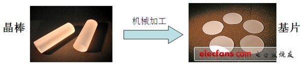
First of all, for the sapphire substrate, it has undergone several processes from cutting, rough grinding, fine grinding, and polishing before becoming a qualified substrate. Take the 2-inch sapphire as an example:
1. Cutting: Cutting is cutting from sapphire ingots to wire pieces with a thickness of about 500um by a wire cutting machine. In this process, diamond wire saw is the most important consumable, currently mainly from Japan, South Korea and Taiwan.
2. Rough polishing: The surface of the sapphire after cutting is very rough, and it needs to be rough polished to repair the deep scratches and improve the overall flatness. This step mainly uses 50 ~ 80um B4C plus Coolant for grinding. After grinding, the surface roughness Ra is about 1um.
3. Fine polishing: The next step is more elaborate processing, because it is directly related to the yield and quality of the final product. The thickness of the currently standardized 2-inch sapphire substrate is 430um, so the total removal of fine polishing is about 30um. Taking into account the removal rate and the final surface roughness Ra, this step is mainly to process the polycrystalline diamond solution with the resin tin plate in a Lapping manner.
In order to pursue stability, most sapphire substrate manufacturers use Japanese grinding machines and original polycrystalline diamond liquid. However, with the rising cost pressure and the improvement of the domestic consumables level, domestic consumables products can now replace the original products, and significantly reduce costs.
Speaking of polycrystalline diamond liquid, you may wish to say a few words. For the fine powder part of polycrystalline diamond liquid, it is generally required that the particle size is concentrated and the shape is regular, so that it can provide long-lasting cutting force and the surface scratches are relatively uniform. Domestic manufacturers of polycrystalline diamond fine powder include Beijing Guoruisheng and Sichuan Jiuyuan, while Guoruisheng can also produce diamond liquid by itself, so it has great advantages in quality and cost. Diamond InnovaTIon of the United States recently launched a "polycrystalline diamond", which is actually an improvement on ordinary single crystal diamond. Although the stronger structure can provide higher cutting force, it is also more likely to cause deep scratches. .
4. Polishing: Although the scratches caused by polycrystalline diamonds are significantly smaller than those of single crystal diamonds, they will still leave obvious scratches on the surface of the sapphire, so it will undergo a CMP polishing to remove all scratches and leave a perfect surface . The CMP process was originally a process for planarizing silicon substrates, and is now also applicable to sapphire substrates. The sapphire substrate after the CMP polishing process is inspected layer by layer, and the products that meet the qualification criteria can be handed over to the epitaxy plant for epitaxy.
Second, the thinning process of the back of the chip
After the epitaxial sapphire substrate becomes an epitaxial wafer, after the epitaxial wafer undergoes a series of complex semiconductor processes such as etching, evaporation, electrode production, and protective layer production, it needs to be cut into a grain of chips. According to the size of the chip, A 2-inch epitaxial wafer can be cut into thousands to tens of thousands of CHIPs. As mentioned above, the thickness of the epitaxial wafer is around 430um at this time. Due to the hardness and brittleness of sapphire, it is difficult to process it by the ordinary cutting process. The current common process is to reduce the epitaxial wafer from 430um to around 100um, and then use laser to cut.
1. Grinding process:
Although the processing quality of epitaxial wafers is good by Lapping, the removal rate is too low, and the maximum can only reach about 3um / min. If Lapping is used throughout the process, this processing will take about 2h, and the time cost is too high . The current solution is to join the Grinding process before Lapping, and to achieve the purpose of rapid thinning through the cooperation of the diamond grinding wheel and the thinning machine.
2. Lapping process
After thinning, use about 6um polycrystalline diamond liquid with resin copper disc, which can not only achieve a higher removal rate, but also repair the deep scratches left by the Grinding process. Generally speaking, the cracks in the cutting process are due to the deep scratches in the Grinding process that have not been removed, so the requirements for diamond fluid are also relatively high at this time.
In addition to splits, in order to increase the brightness of the chip, some chip manufacturers will also plate copper on the back of the epitaxial wafer after the Lapping process. At this time, higher requirements are placed on the surface after Lapping. Although some scratches will not cause slivers, it will affect the effect of back plating. At this time, 3um polycrystalline diamond liquid or smaller fineness can be used for the Lapping process to achieve better surface quality.
Round Industrial Lighting LED Driver
MOSO Round Industrial Lighting LED Driver has programmable output current. It is a brilliant design with advanced technologies. It`s designed for external assembling of round shape LED light fixtures, like round high bay, low bay lights, or flood lights, canopy lights, or horticulture lights used in industrial area, or factories, warehouses, and greenhouses.


The round industrial lighting led driver got global safety certifications, including UL, CE, TUV, CB, SAA, BIS, KC, etc. The LED control gear has universal input voltage, from 90~305Vac. It is a reliable product compatible with various application and different countries.
The perfect cooling design can ensure the product reliability and long lifetime for at least 10 years (50,000hours operation at least) minimum.
MOSO grants the product with 5 years global warranty. Customer can refer to Warranty policy, find the closest MOSO distributors or sales representatives, to get a local replacement in case of any failure.
Drivers with dimming 0~10V & PWM is available.
Round Industrial Lighting LED Driver
Round Industrial Lighting LED Driver, Round Industrial Led High Bay Light Driver,Waterproof Industrial LED Driver,Flicker Free Round LED Driver
Moso Electronics , https://www.mosoleddriver.com